 |
 |
| Introduction | construction-1 | Construction-2 | Construction-3 |
NoteThis " 6 Digit Frequency Counter " circuit and PCB was designed by Laurier Gendron. It is being made available to hobbyists for personal development only. It cannot be used for commercial purposes of any kind without previous written permission. ( 10 Feb.2001 )
Introduction
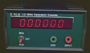
Based on the application of the three digit decoder driver chip MC14553 published in the Motorola data manual I undertook the task of designing a 6-digit frequency meter and the results were excellent , simple enough and at a cost of well under $ 50.00 Canadian.
Since the Frequency counter may require as much as 250ma of current when all digits are illuminated it was designed as a bench instrument complete with a regulated power supply as described later. The transformer used was retrieved from an ancient digital alarm clock . Although a clocking signal could have been derived from the AC supply line , a digital clock oscillator was incorporated into the design to accommodate a battery pack supply instead of an AC supply source as an alternative. .
Following the design application of the Digital Capacitance Meter , the digital display read out section needed to be expanded by adding a second set of three digits for a total of six digits to accomplish my goal of being able to count up to 1 Mhz without adding many stages of frequency division .
Once this accomplished I decided to increase the capability by adding one dividing stage to obtain a reading up to 12 Mhz and this was accomplished by adding only on IC and one switching stage .
You can make a search and download application data sheets for all the IC's used in this project from MotorolaThe circuit
In addition to the six digits counter circuit for display , the measurement of a frequency can be achieved with only four additional CMOS IC's ,MC or CD4521, 2 - MC or CD4093 and one MC or CD4017 . The six digits counter is made of two CMOS IC's MC14553 and two MC or CD14543 , six common Cathode digital displays and a few other parts . A complete list of parts is provided .
Logic Circuit Description
As a reference you may wish to open up a new window to view the circuit while reading the description.( The window size is adjustable)
a ) Condition the input stage to accept a sine, square, pulse or triangle signal.
b ) Amplify a weak signal voltage to a level required for good processing.
c ) Attenuate any high level signal to a pre-determined level so as not to overload the permissible logic input voltage level .
d ) Shape most frequency signals to be acceptable by the counter section for stable processing .
e ) Provide for a timing sequence interval to enable the counter to accumulate a total count that accurately reflects the frequency being measured.The input is fed to Q1 through R8 . Q1 is configured to amplify or attenuate the input signal and delivers a square wave from its collector output to pins 8 and 9 of IC-3 then this square wave is shaped into a pulse by two of the four gates available of IC-3 circuit , R5 and C5 also form part of that shaping circuit which is similar to the one shown in more details for IC-2 .
The output of IC-3 is taken from pin 11 and its one output is all that is require for a maximum count of 999,999 hertz which in this case can be connected directly to IC-2 gate D pin 13.
To obtain a count of more than 1 MHz, IC-4 CMOS 4017 is added to enable us to count up to 12 MHz which is the maximum operating frequency of IC-4 .The output of IC-3 from pin 11 is also sent to IC-4 pin 14 , IC-4 is used as a frequency divider and is configured to divide any frequency by 10 , thus for a given frequency of 10 MHz the counter will register and display 100,000.
Switch S1 is used to select the output of either IC-3 for a maximum count of MHz ( 999,999 ) or the output of IC-4 for a count of up to 12 MHz which in this case would be displayed as 120,000 .The selected output is fed to the input of gate D of IC-2 as mentioned earlier , IC-2 is used to shape all the input signals required by the three digit counters CMOS MC14553 described below .
In order to be able to provide timing pulses to the counter an oscillator is required , IC-1 CMOS 4521 with its appropriate crystal (see parts list - xtal ) delivers a one ( 1 ) pulse per second taken from pin 15 and is delivered to pin 1 & 2 of gate A and pin 12 of gate D of IC-2 .As we can see IC-2 and IC-3 are used with the combination of C3,C4,C5,R3,R4 ,R5 to condition and invert the pulses where required to the counter as it requires exact timing and pulses shape for the stable operation of the counter.
The Counter Display
As a reference you may wish to open up a new window to view the circuit while reading the description.( The window size is adjustable )
To do this the MC14553 needs three input signals, a positive (high) pulse to the Latch input ( pin #10 ) to enable storage of pulses to be stored into the latch and a Reset ( pin # 13 ) pulse ( high ) to reset the counter . The total count desired is controlled by the Latch action which sets the time we require to insert the amount of pulses to the Counter ( pin #12) to be displayed.
When the latch is high the count starts and when the Latch is low (zero) the count is stopped and the total of pulses accumulated in the latch are displayed then a positive pulse is required to the Reset to clear the Latch , the speed of this process is controlled by an internal 100 kHz oscillator which is determined by the .001 capacitor C7 connected between pin # 3 and pin # 4 of IC-6 .
To display six ( 6 ) digit we simply add an exact duplicate of the three digit circuit and connect the overflow from pin 14 of IC-6 to pin 12 of IC-5 as well as carry the oscillator signal from pin 3 of IC-6 to pin 4 of IC-5 and duplicate the inputs of the " Count, Reset, Latch " as well.
Notice that only one set of driving transistors of three is still used but they are now connected to the second set of digit as well BUT the segment connections of each three digit must be kept separate and connected to its dedicated digit driver IC-7 and IC-8 as shown.
Introduction construction-1 Construction-2 Construction-3
If you have any comments or questions email me at roma60@home.com © Laurier Gendron, Burnaby, B.C., Canada. 1998

