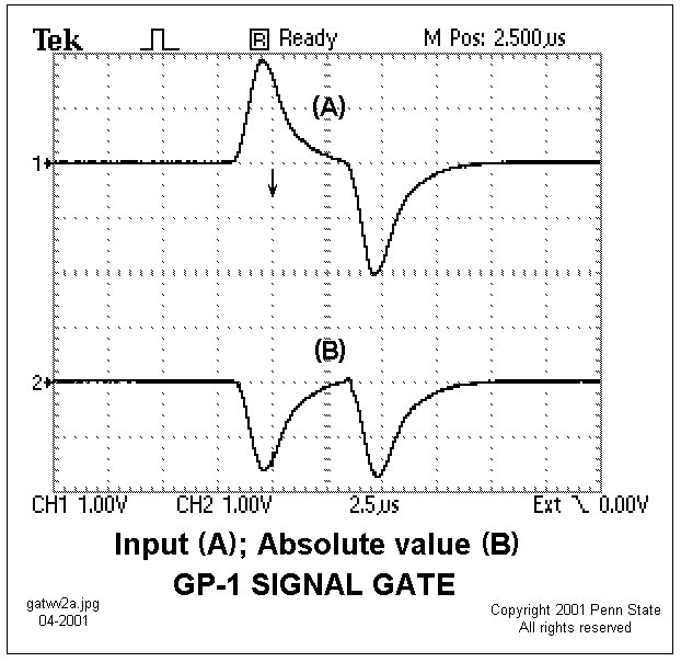
 Biphasic input signal from the
Simulator seen at point (A) on the Signal
Gate circuit diagram. The inverted absolute value is found at
(B) and clearly shows the absolute value circuit behavior of converting
input signals of either polarity into single polarity waveforms.
Biphasic input signal from the
Simulator seen at point (A) on the Signal
Gate circuit diagram. The inverted absolute value is found at
(B) and clearly shows the absolute value circuit behavior of converting
input signals of either polarity into single polarity waveforms.