The ( double - sided ) PC board was designed using ExpressPCB CAD, and measures 2.5 x 3.8 inches. A schematic diagram of the circuit is provided near the bottom of this page. If you choose to purchase the PC board from ExpressPCB, ( or me ) the board will have “through plated” holes, so there will be no need to install wire jumpers in the “vias”.
The component density is very high on this board, but I managed to provide some uncommited pads near the PIC chip, which will allow a 16 - conductor ribbon cable to be installed, to connect signals between the PIC and / or MicroMint chip, and the “outside world”. The board size was limited to 2.5 x 3.8 inches because that is the ONLY size allowed by ExpressPCB for their “Mini Board” service, which is the most economical ( small quantity ) service they offer.
Although the artwork is provided in this section of the website, I HIGHLY reccomend ( if you don't get a board from me ) using the CAD file and the ExpressPCB web service... Most of the tracks are only 0.012 inch wide, ( VERY hard to etch at home ) and there are dozens of “vias” that would require the installation of a ( through board ) wire jumper, if the board is made with ordinary “hobby” PCB methods.
The ExpressPCB website offers their CAD program for free, and it can be downloaded ( about 3.7 megabytes, total ) at their website :
The CAD is modest, but highly intuitive, and adequate for most tasks... It has a ( modest ) library of “footprints” for a vareity of common devices. I have used their service a few times now, and have never found their work to less than flawless.
Once you have downloaded and installed the ExpressPCB CAD program, you can use it to examine ( and submit for purchase ) the CAD file for this computer’s PC board, which is available here :
For those who choose to use the ExpressPCB service for other types of PC boards, but think they need more features in the CAD program, I should mention that the CAD software was written by IVEX, which offers WinBoard to do the same task... they have collaborated with ExpressPCB to achieve this, and WinBoard ( which has many extra features, for a modest price ) offers the same “web based” submission service. I have never tried it, but I do use an older version of IVEX WinBoard for all the other artwork on this website. Their website is located at :
If you INSIST on making your own boards, you can find the photo artwork in the section called SBC_DRAWINGS. The artwork was "captured" from the CAD display screen using a crude method, causing many of the PCB tracks to appear "jagged" or "rough"... the actual boards are MUCH cleaner. A parts pictorial drawing is also provided, showing the location of the ( various ) components. ( pictorial information is automatically included in the CAD file, as well )
THE CIRCUIT
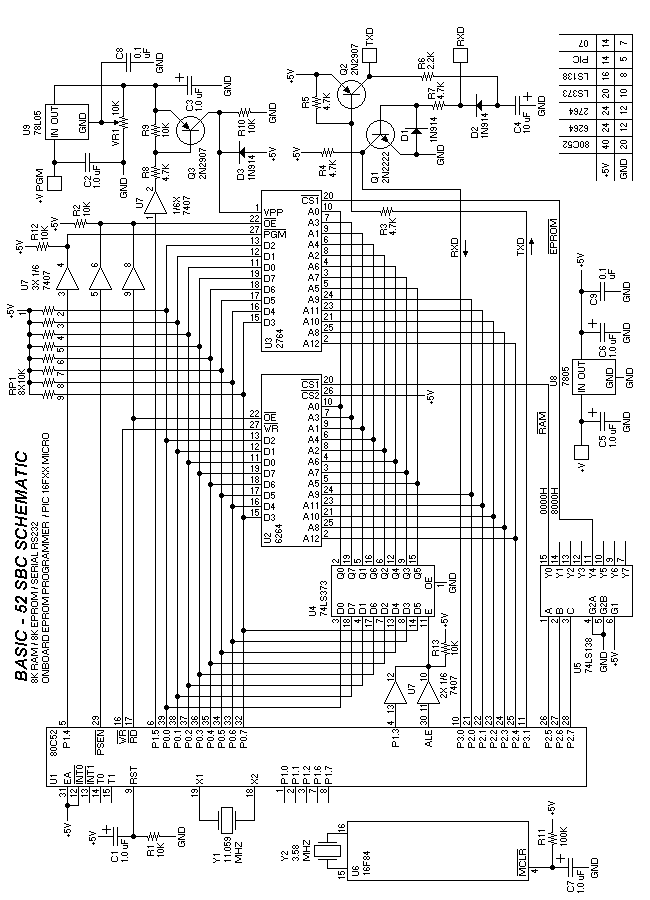
Here is the schematic diagram of the BASIC - 52 SBC. The vertical orientation simplifies a "hardcopy" printout from a web browser. If you want to see a horizontal version of the schematic, click [ HERE ].
The "unprogrammed" version of the 80C52 is basically designed to provide 4 parallel ports, with 8 bits per port. The BASIC - 52 interpeter uses most of them, so the pin definitions and names ( in this circuit here ) are "defined" by the interpeter. Negative voltage for the RS232 TX port is "robbed" from the host computer's RS232 port, by diode D2 and capacitor C4. BASIC - 52 requires a minimum of 1K of RAM to "sign on" and run. The EPROM programmer operates on EPROMS starting at hex address 8000.
You may notice that several of the address and data lines for the micro, RAM and EPROM do not "agree" with each other... For example, data line "D0" on the micro ( = P0.0, pin 39 ) runs to data line "D2" ( pin 13 ) on the RAM and EPROM chips... this was done as a matter of convenience for PCB layout, and has no effect on the operation of the computer... The "names" of these pins is really pretty "arbitrary" anyway, and this design demonstrates that fact. The only consequence would be if EPROMS from this computer were installed in some other BASIC - 52 computer, in which case they would not work.
Programming voltage for the EPROM is provided by U9, and can be adjusted by VR1, since EPROMS are available with a vareity of different Vpp voltages. The Vpp supply is provided with a separate input pad, since Vpp will only be required when an EPROM is actually programmed. Vpp should probably be applied after the computer has booted up, to ensure that the EPROM is not "accidentally" programmed ( with a few bytes of random data ) while the computer is starting up. ( I have not seen this problem, but I suppose it is possible )
Pin 12 ( P3.2 ) is tied high in this design, but it can be used by an EEPROM to "slow down" the programming speed of the BASIC - 52 EPROM programming routine, in case a "slow" EEPROM is used... some EEPROMs have a pin that generates a "WAIT status" signal, that can be tied to this pin. Otherwise, this pin must be tied high.
U7 is an open - collector hex buffer, and requires an external pull-up resistor on each output to generate a logic "high" signal. The pull-ups can be tied to voltages as high as 30 volts, so U7 is ( mainly ) used here to translate signals from TTL levels to higher voltage levels, required by the EPROM. Open collector outputs also allows multiple outputs to be tied together in parallel, to achieve a logic "AND GATE" function. This is done for the outputs on pins 6 and 8, as well as pins 10 and 12.
Due to the limited number of pins on the chip, the bottom 8 bits of memory address are "time shared" with the 8 bits for the data bus, on pins 32 through 39. Before each memory access ( either read or write ) is performed, the bottom 8 bits of address are applied to these pins, and "latched" into U4 by a pulse applied to U4-11. Decoding for the memory chips is provided by U5.
If you want to add more memory to this design, the easiest way ( but not the cleanest ) is to simply install the extra EPROM or RAM chips directly on top of the original chips, ("piggy back") and solder the pins together, but leave pin 20 on the new chips DISCONNECTED from pin 20 on the original chips. Pin 20 on the new chips can then be "hand wired" to the "unused" outputs of U5, to provide the new chips with their own (unique) addresses... use U5 pins 14, 13 and 12 (in that order) for extra RAM chips, ( maximum RAM = 32K ) and use U5 pins 10, 9 , and 7 ( in that order ) for extra EPROM chips. ( maximum EPROM = 32K )