VCO Phase noise
Characterizing Phase Noise
The term phase noise is widely used for describing short term random frequency fluctuations of a signal. Frequency stability is a measure of the degree to which an oscillator maintains the same value of frequency over a given time. This may be specified in a number of ways. Three commonly used terms for describing frequency stability are used here. An ideal sine wave oscillator may be described by
-
V(t) = VoSin2Pft
-
V(t) = Vo {1 + A(t)} Sin {2P ft + q (t)}
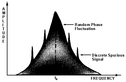
Figure 1

Spectrum analyzer display of phase noise
The source of phase noise in an oscillator is due to thermal and flicker or 1/f noise. Most
oscillators operate in saturation. The AM noise component is usually 20dB lower than the phase
noise component. In the discussion that follows, we will assume that A(t)<<1.
Many methods are used to characterize phase noise of an oscillator. Essentially, all methods
measure the frequency or phase deviation of the source under test in either frequency or time
domain. Since frequency and phase are related to each other, all these terms are also related. One
of the most common fundamental descriptions of phase noise is the one sided spectral density of
phase fluctuations per unit bandwidth. The term spectral density describes the energy
distributions as a continuous function, expressed in units of energy per unit bandwidth. The
phase noise of an oscillator is best described in the frequency domain where the spectral density
is characterized by measuring the noise sidebands on either side of the output signal center
frequency. Single sideband phase noise is specified in dBc/Hz at a given frequency offset from
the carrier. The frequency domain information about phase or frequency is contained in the
power spectral density SDq(f) of the phase or in the power spectral density SDf(f) of the
frequency. Here, f refers to the modulation frequency or offset frequency associated with the
noise-like variations in q(t).
Peak phase modulation Dq and peak frequency modulation Df are related as follows:


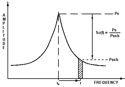
Figure 2

One sided representation of phase noise spectral density of signal
Similarly, one sided spectral distribution of the frequency fluctuations per Hz bandwidth is SDf (f) where
- SDf = (Dfrms)2 / BW
SC(f) = (Power density in one sideband per Hz bandwidth at an offset frequency f away from the carrier) / (Total signal power)
For small phase fluctuations, we can write


Sc(f) = 1/2 (SDq(f))

Figure 3

Single sideband phase noise to carrier ratio
The Single Sideband Phase Noise is usually given logarithmically, that is:
SC(f) in dB = 10 x log[SC(f)]
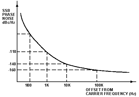
This is shown in Figure 4 as a spectral density plot of the phase modulation sidebands in the frequency domain. It is expressed in dB relative to the carrier per Hz bandwidth.
Figure 4

Single sideband phase noise representation
The phase noise generated by a VCO is determined by:
- (a). Q factor of the resonator.
(b). Q of the varactor diode.
(c). the active device used for the oscillating transistor.
(d). power supply noise.
(e). external tuning voltage supply noise.
The noise contribution made by (d) and (e) can be minimized by careful choice of the power
supplies (see Application Note 3). The phase noise of the VCO is therefore determined primarily
by the overall Q of the circuit. In order to design a circuit with high Q, the tuning bandwidth
must be made small. Therefore a VCO designed for low phase noise performance will have a
smaller tuning range.
Ways to minimize noise
The following steps are recommended for obtaining the best overall performance from Mini-Circuits VCO's.
1. Power Supply (Vcc) and tuning voltage (Vtune) returns must be connected to the printed circuit board ground plane. VCO ground plane must be the same as that of the printed circuit board and therefore all VCO ground pins must be soldered direct to the printed circuit board ground plane.
2. Adequate RF grounding is required. Several chip decoupling capacitors must be provided between the Vcc supply and ground.
3. Good, low noise power supplies must be used. Ideally, DC batteries for both supply (VCC) and tuning (V tune) voltages will provide the best overall performance.
4. Output must be correctly terminated with a good load impedance. It is also a good practice to use a resistive pad between the VCO and the external load.
5. Connections to the tuning port must be as short as possible and must be well screened, shielded, and decoupled to prevent the VCO from being modulated by external noise sources. A low noise power supply must be used for tuning voltage (Vtune) Supply.