HELA-10, High IP3, Wide band, Linear Power Amplifier
1.0 Introduction
Communication systems are becoming increasingly complex. Number of carriers used in systems such as CATV is constantly increasing. This complexity increases the inter-modulation products. In order to keep the inter-modulation products under control, the carrier levels need to be lower or the system power output needs to be increased.
Increased output power results in a corresponding increase in DC power consumption and cost. Feed forward amplifiers are used extensively to increase inter-modulation intercept point and thereby decrease the inter-modulation products. Feed forward amplifiers are generally expensive and are not easily available. This product feature presents a new device, HELA-10 which uses a set of balanced amplifiers, which provide high intercept point comparable to feed forward amplifier but at a significantly lower cost.
2.0 HELA-10, A Balanced Power Amplifier
HELA-10 is a balanced, sixteen lead, power amplifier with a nominal gain of 11 dB. Figure 1 shows a photograph of the amplifier. Figure 2 shows the layout of the amplifier with external baluns. It is powered by a single, +12V DC power supply. It operates in Class-A and produces a nominal output power of 1 Watt.
HELA -10 consists of a pair of amplifiers. As they are on the same chip, their gain and phase are very well matched. If a balanced signal is applied to its input, then its output produces a balanced output. By using a set of Baluns at the input and output (Figure 3), a single ended input is first converted into a balanced output in Balun #1, amplified in the amplifiers #1 & #2 and combined in the Balun #2 to produce a single ended output. If the loss of the output balun is zero, the amplifier pair can produce twice the output power of a single amplifier.
Amplifiers are nonlinear. The degree of non-linearity of an amplifier depends on how hard they are driven. Now let us look at the harmonics generated by the amplifier. The phase of the harmonics is related to the phase of the fundamental signal at the input of the amplifier. Let us look at the second harmonic (Figure 4.), the phase at the output is the same. Hence, they get canceled and a second harmonic does not appear at the output of the amplifier. The same is true for all even harmonics. In reality, the amplifiers and baluns are not perfect, hence a small amount of signal is present. HELA-10 has an excellent second order intercept of 88 dBm typical. As the two amplifiers are combined, the power output and odd order intercept point are twice that of the single amplifier.
3.0 Specifications and Performance
Table 1 shows the electrical specifications of the amplifier at room temperature. As can be seen, the power output is typically 30 dBm. A unique feature of this amplifier is its ability to work in both 50 and 75 ohm systems. Mini-Circuits supplies separate sets of Baluns for 75 ohm (MCL part number ADTL1-18-75) and 50 ohm (MCL part number ADTL1-12) systems. Figure 5. Shows the gain and Figure 6 the VSWR of HELA-10 in a 75 ohm system. Gain is extremely flat and it is typically within ±0.4 dB. This is an exellent feature for wideband systems. The VSWR is typically, 1.2:1 showing an excellent match. This meets the stringent matching requirements of a CATV amplifier. Figure 7 shows the output power and Figure 8 the output third order intercept point. Output power is typically 30 dBm (1 watt) over the entire band. IP3 of amplifiers is in general, 10 dB above 1 dB compression. For HELA-10, IP3 is typically 16 dB above 1 dB compression at 150 MHz and 14.7 dB above it at 800 MHz. This is equivalent to using 5 watt amplifier at 150 MHz and 3 Watt at 800 MHz. This high IP3 is of great advantage for use in multi carrier systems.
Figure 9-12 shows the same parameters; Gain, VSWR, Output Power and Output IP3 with 50 S matching circuits. As it can be seen, the gain is very similar to the 75 ohm system and is very flat. Port matching is excellent above 300 MHz and is typically 1.2:1. Below 300 MHz, the VSWR increases to a manageable 2:1. Power output and IP3 are comparable to the 75 ohm version. At cellular frequencies, this amplifier has an excellent IP3 of 45 dBm and delivers 1W of power and excellent port matching. This makes it a superb amplifier for cellular frequencies.
All the referenced graphs and conclusions cover the entire circuit which includes the baluns and the biasing circuits described in 4.0. This amplifier along with the transformers housed in surface mount package makes it an ideal candidate suitable for pick and place and high volume production.
4.0 Performance of HELA-10 as a Cascaded Amplifier
For higher gain applications, a driver amplifier is required. It may not be easy to find a driver having sufficiently high IP3 since the driver contributes to the overall IP3. HELA-10 is a cascadable amplifier. Hence it can also be used as a driver. Figure 13 shows the schematic block diagram of a two stage, cascaded HELA-10 amplifier. A typical gain of 20 dB gain can be achieved using this cascade.
The disadvantage of a direct cascade is the power consumption, which is twice that of a single amplifier. But, HELA-10 has an intelligent biasing scheme to overcome this. By connecting an external shunt resistance from pin #7 to ground the supply current can be controlled. Figure 14 shows the supply current of the amplifier as a function of shunt resistance, which shows the current can be reduced to almost half. Figure 15 shows the 1dB compression versus shunt resistance. Figure 15-1 & 15-2 show Pout at 4 different frequencies vs. shunt resistance and Figure 15-3 & 15-4 show Pout as a function of frequency. A bias resistor value in the range of 10 to 100 ohms reduces the current consumption by 150 to 200 mA and still produces a power output of 27 dBm typically. This is more than adequate as a driver. This feature can also be used to reduce the current consumption when HELA-10 is used for lower power applications. Figure 16-1 and 16-2 show the performance (Gain) over 50 to 1000 MHz using various shunt resistances in 75 ohm and 50 ohm systems. Figure 17-1 and 17-2 show IP3 at various values of shunt resistance in 75 & 50 ohms respectively. As seen in Figure 16-2, the gain variation is very small, about 0.3 dB. But the output power can be reduced and also the supply current using a standard 1/8 watt resistor.
HELA-10 can also be used at different supply voltages, at customer's discretion. Figure 18 shows the DC current at various supply voltages. Figure 19-1 and 19-2 show the output power in 75 and 50 ohm systems at various supply voltages. Figure 20-1 and 20-2 show the Gain at various supply voltages. Figures 21-1 and 21-2 show the IP3 at 800 MHz at various supply voltages. Table 2 shows a summary of the findings in electrical specifications both in 50 ohm and 75 ohm systems.
5.0 Layout and Thermal Aspects:
The PCB layout for the HELA-10 amplifier must consider both the electrical requirements of the parts (proper line impedance, bypassing, etc.) and the thermal requirements. The thermal requirement, to meet the stated MTTF of better than 800 years, states that the maximum temperature of the heat slug on the bottom of the HELA-10 package is 110°C. There are three different thermal interfaces between the bottom of the HELA-10 and the chassis. The first is the solder connection of the HELA-10 heat slug to the PCB. The second interface is the heat transfer through the PCB, and the third is the PCB to chassis interface.
The first interface, the solder connection of the HELA-10 heat slug to the PCB, should cover the full area of the HELA-10 heat slug for maximum effectiveness.
The PCB must be designed for the maximum expected system ambient temperature. To do this, the following two parameters need to be known: the maximum external ambient temperature and the temperature rise of the chassis above the external ambient temperature.
Once these two parameters are known the maximum temperature rise between the chassis and the HELA-10 can easily be calculated.
| Maximum Temperature Rise (°C): | Chassis to HELA-10 slug = 110 - maximum external temperature - chassis rise |
| For example if: | Maximum external temperature = 60°C Chassis rise due to internal heating = 20°C |
| Then: | Maximum Temperature Rise (°C): Chassis to HELA-10 slug = 110 - 60 - 20= 30°C |
In the above example a 30°C rise is allowed in the PCB mount between the bottom of the HELA-10 slug and the chassis. Knowing this a PCB can be designed that provides a thermal resistance which will maintain a 30°C or less temperature rise.
The second interface is the heat transfer through the PCB. FR4, the typical PCB material used in most applications, has very poor thermal conduction properties and cannot be used without the addition of through via holes under the HELA-10. The via holes should be copper plated and then solder filled for the lowest thermal resistance. The via holes then conduct the heat through the FR4 to the bottom of the PCB, while the FR4 material provides the mechanical support. The thermal resistance of the via holes, given in degree C rise per watt of power dissipation, is a function of via diameter and the thickness of the copper plating on the walls of the via holes. Tables 3, 4, 5 show the calculated thermal resistance of solder filled, plated though via hole with different via diameter and copper plating thickness. Table 3 shows the thermal resistance with 0.8 mil copper plating, Table 4 with 1 mil, and Table 5 with 2 mil copper plating. The thermal resistance of the copper plating alone is shown in the column Plating, the thermal resistance of the solder fill is shown in the next column and the column labeled combined shows the calculated thermal resistance of both the copper plating and the solder fill for a single via. The next columns show the thermal resistance achieved by using multiple via holes.
As an example, a 32 mil diameter via with 2 mil thick copper plating has the following properties:
Thermal resistance of the copper plating = 32.5°C / watt
Thermal resistance of the solder fill = 77.7°C / watt
Combined thermal resistance of Single Via, a parallel combination of the above = 22.94°C / watt
A thermal resistance of 22.94°C / Watt would produce a 145°C rise with 6.3 Watts of power dissipation (HELA-10) and therefore a single via cannot be used. As more via holes are added, the combined thermal resistance decreases quickly and is determined the same way as for parallel resistors. If we use 36 such via holes the total thermal resistance will be only 0.64°C per Watt and the temperature rise though the PCB will be only 4°C. The actual via diameter, thickness of the copper plating, and number of via holes used will be determined by the limits of the PCB manufacturing process used.
The third interface is between the PCB and the chassis. Note the chassis is considered to be an infinite heat sink in this application note. Unlike the HELA-10 to PCB interface, this cannot be a solder connection due to the mismatch in thermal expansion of the PCB and chassis material and other production problems. A thermally conductive elastomer or gasket material is recommended. One such material that maybe applicable for this application is Thermagon, Inc.'s T-PLI 200 material. This material is a thermally conductive, conformable elastomer that is available in either sheet form or cut to size.
This material should conform to any irregularities on the PCB and chassis surfaces cause by the manufacturing process while providing a low thermal resistance. A sheet thickness of 20 mils appears to be the best compromise between thermal resistance, tolerance build-up, and handling. The 20 mil thick material has a stated thermal resistance of 0.14°C - in2 per Watt. Using a square area of 0.1 square inches at this interface and a power dissipation of 6.3 Watts a temperature rise of 8.8°C is expected. The PCB should be attached to the chassis with screws, providing a slight compression of the elastomer material. The user must determine if this material is acceptable for their application.
By excellent thermal management technique, HELA-10 is kept at less then 110°C. Hence it can be soldered to the PCB with normal solder such as SN60 or SN63 and also can be used at max. ambient temperature of 80°C.
6.0 Environmental Capabilities
As part of qualification, testing HELA-10 amplifier in its 16-lead SOIC
package has passed the following environmental tests under the conditions
listed below:
| Test | Specification | Conditions | Units Passed/failed |
| Temperature Cycling with Pre-stress | Jedec-Jes22 Method A112 (Pre-stress) |
85°C/85°C, 72 hours 230°C peak reflow | 90 / 0 (2 lots) |
| MIL-STD-883 Method 1010 (Temp Cycle) | -65°C to 165°C 100 cycles Air to Air | ||
| Accelerated Humidity HAST | Jedec-22-A110 without bias | 125°C/85%RH 72 hours | 90 / 0 (2 lots) |
| Thermal Shock | MIL-STD-883 Method 1011 | -55°C to 125°C 15 cycles Liquid | 78 / 0 (2 lots) |
| Autoclave | Jedec-Jesd22 Test Meth. A102B | 121°C/100%RH 72 hrs. | 90 / 0 (2 lots) |
| Solder Reflow Heat | ---- | One pass belt furnace 220°C peak | 90 / 0 (2 lots) |
7.0 Conclusion
HELA-10 is a versatile one watt high IP3 (45 dBm) and IP2 (88 dBm) low cost monolithic amplifier. External baluns are required. Balun sets as well as amplifier test boards are offered by Mini-Circuits. The amplifiers are cascadable and perform equally well in both 75 ohms and 50 ohms system. HELA-10 can also be used as a high IP3 low power driver amplifier with reduced maximum power out capability. As a driver, it has a low current mode built into its biasing circuit in order to reduce DC power consumption.
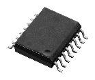
Figure 1 - HELA 10 Photograph
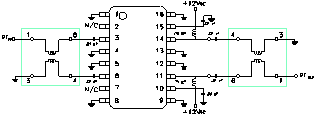
Figure 2 - HELA 10 Layout with External Baluns
-
.01 µ
F Cap is Mini-Circuits Part Number B55-11-103
.75 µ H Choke is Mini-Circuits Part Number B65-C5-751JC
Table 1 - Electrical Specifications at 25�C
|
FREQ (MHz) |
GAIN* (dB) |
MAXIMUM POWER (dBm) Output Input (1dB Comp.) (no |
DYNAMIC RANGE NF IP3 dB dBm |
VSWR*** Typ (:1) |
DC POWER |
THERMAL RESISTANCE** |
||||||||
|
Min. |
Typ |
Max |
Typ Flatness |
Typ |
Min |
damage) |
Typ |
Typ |
In |
Out |
Volt (V) |
Current (mA) |
0jc �C/W |
|
|
50-1000 |
10 |
11 |
13 |
�0.4 |
30 |
26 |
20 |
3.5 |
47 |
1.22 |
1.22 |
12 |
525 |
6 |
-
* Includes transformer losses at input and output.
** Thermal resistance form junction to heat slug.
*** For 75 ohm. For 50 ohm. VSWR increases from 1.2:1 at 1 GHz to 2.0:1 at 50 MHz.
Table 2
|
HELA-10 |
50 Ohm System |
75 Ohm System |
|
Gain vs. Shunt Resistance |
Gain variation with shunt resistance is minimal and is 0.3 dB typical. |
Gain variation with shunt resistance is minimal and is 0.3 dB typical. |
|
Pout vs. Shunt Resistance |
There are 1.5 dB and 2.4 dB improvement on Pout for both low and high frequency range from 10 to 100 ohm and 100 to 1000 ohm Shunt Resistance. Above 1000 ohm Shunt resistance, Pout is almost the same. |
There are 1.3 dB and 2.1 dB improvement on Pout for both low and high frequency range from 10 to 100 ohm and 100 to 1000 ohm Shunt Resistance. Above 1000 ohm Shunt resistance, Pout is almost the same. |
|
OIP3 vs. Shunt Resistance |
IP3 increases with increasing shunt resistance (Figure 11). |
IP3 increases with increasing shunt resistance (Figure 11). |
|
DC Supply Current vs. Shunt Resistance
|
Current increases with increasing shunt resistance and varies from 250 to 450 mA (Figure 14). |
Current increases with decreasing shunt resistance and varies from 250 to 450 mA (Figure 14). |
|
Gain vs. Supply Voltage |
Gain variation is 0.5 to 1.0 dB from 5 volts to 13 volts. |
Gain variation is 0.5 to 1.0 dB from 5 volts to 13 volts. |
|
Max. Pout vs. Supply Voltage |
Max. Pout increases from +22 dBm to +32 dBm for device voltages from 4 volts to 13 volts DC. |
Similar to 50 ohm system. |
|
DC Current vs. Supply Voltage |
DC current is proportional to supply voltage. |
Similar to 50 ohm system. |
|
OIP3 vs. Supply Voltage |
OIP3 increases with supply voltage. |
Similar to 50 ohm system. |
|
VSWR ( Input ) |
Decreases from 2.6:1 at 50 MHz to 1.2:1 at 300 MHz and beyond. |
Very low, 1.2:1 over the entire range |
|
VSWR ( Output ) |
Decreases from 2.6:1 at 50 MHz to 1.2:1 at 300 MHz and beyond. |
Very low 1.15:1 over the entire range. |
Table 3 - Thermal Resistance of Solder Filled, Plated Thru Via Hole
| 62 mils | |
| 0.8 mils | |
| 3.98 Watts/cm�C | |
| 0.51 Watts/cm�C |
| Via | Thermal Resistance (�C/Watt) |
Multiple Vias |
|||||||
| Dia (Mils) | Plating | Fill | Combined | 10 | 20 | 30 | 40 | 50 | 60 |
|
10 11 12 13 14 15 16 17 18 19 20 21 22 23 24 25 26 27 28 29 30 31 32 33 34 35 36 37 38 39 40 41 42 43 44 45 46 47 48 49 50 |
265.2 239.2 217.9 200.0 184.9 171.8 160.5 150.6 141.9 134.1 127.1 120.8 115.1 109.9 105.2 100.8 96.8 93.1 89.7 86.5 83.6 80.8 78.2 75.8 73.5 71.4 69.3 67.4 65.6 63.9 62.3 60.7 59.2 57.8 56.5 55.2 54.0 52.8 51.7 50.6 49.6 |
863.7 689.7 563.4 468.9 396.3 339.4 293.9 257.0 226.6 201.3 180.0 161.9 146.4 133.1 121.5 111.3 102.4 94.5 87.4 81.2 75.6 70.5 65.9 61.8 58.1 54.6 51.5 48.6 46.0 43.6 41.3 39.3 37.3 35.6 33.9 32.4 30.9 29.6 28.3 27.1 26.0 |
202.92 177.62 157.12 140.21 126.06 114.08 103.83 94.96 87.24 80.47 74.49 69.19 64.45 60.20 56.37 52.90 49.76 46.90 44.28 41.88 39.68 37.65 35.78 34.04 32.43 30.94 29.55 28.25 27.04 25.90 24.84 23.84 22.90 22.02 21.18 20.40 19.66 18.96 18.29 17.66 17.06 |
20.29 17.76 15.71 14.02 12.61 11.41 10.38 9.50 8.72 8.05 7.45 6.92 6.44 6.02 5.64 5.29 4.98 4.69 4.43 4.19 3.97 3.77 3.58 3.40 3.24 3.09 2.95 2.82 2.70 2.59 2.48 2.38 2.29 2.20 2.12 2.04 1.97 1.90 1.83 1.77 1.71 |
10.15 8.88 7.86 7.01 6.30 5.70 5.19 4.75 4.36 4.02 3.72 3.46 3.22 3.01 2.82 2.65 2.49 2.34 2.21 2.09 1.98 1.88 1.79 1.70 1.62 1.55 1.48 1.41 1.35 1.30 1.24 1.19 1.15 1.10 1.06 1.02 0.98 0.95 0.91 0.88 0.85 |
6.76 5.92 5.24 4.67 4.20 3.80 3.46 3.17 2.91 2.68 2.48 2.31 2.15 2.01 1.88 1.76 1.66 1.56 1.48 1.40 1.32 1.26 1.19 1.13 1.08 1.03 0.98 0.94 0.90 0.86 0.83 0.79 0.76 0.73 0.71 0.68 0.66 0.63 0.61 0.59 0.57 |
5.07 4.44 3.93 3.51 3.15 2.85 2.60 2.37 2.18 2.01 1.86 1.73 1.61 1.50 1.41 1.32 1.24 1.17 1.11 1.05 0.99 0.94 0.89 0.85 0.81 0.77 0.74 0.71 0.68 0.65 0.62 0.60 0.57 0.55 0.53 0.51 0.49 0.47 0.46 0.44 0.43 |
4.06 3.55 3.14 2.80 2.52 2.28 2.08 1.90 1.74 1.61 1.49 1.38 1.29 1.20 1.13 1.06 1.00 0.94 0.89 0.84 0.79 0.75 0.72 0.68 0.65 0.62 0.59 0.56 0.54 0.52 0.50 0.48 0.46 0.44 0.42 0.41 0.39 0.38 0.37 0.35 0.34 |
3.38 2.96 2.62 2.34 2.10 1.90 1.73 1.58 1.45 1.34 1.24 1.15 1.07 1.00 0.94 0.88 0.83 0.78 0.74 0.70 0.66 0.63 0.60 0.57 0.54 0.52 0.49 0.47 0.45 0.43 0.41 0.40 0.38 0.37 0.35 0.34 0.33 0.32 0.30 0.29 0.28 |
Table 4 - Thermal Resistance of Solder Filled, Plated Thru Via Hole
| 62 mils | |
| 1 mils | |
| 3.98 Watts/cm�C | |
| 0.51 Watts/cm�C |
| Via | Thermal Resistance (�C/Watt) | Multiple Vias |
|||||||
Dia (Mils) |
Plating |
Fill |
Combined |
10 |
20 |
30 |
40 |
50 |
60 |
|
10 11 12 13 14 15 16 17 18 19 20 21 22 23 24 25 26 27 28 29 30 31 32 33 34 35 36 37 38 39 40 41 42 43 44 45 46 47 48 49 50 |
216.9 195.2 177.5 162.7 150.2 139.4 130.1 122.0 114.8 108.5 102.7 97.6 93.0 88.7 84.9 81.3 78.1 75.1 72.3 69.7 67.3 65.1 63.0 61.0 59.2 57.4 55.8 54.2 52.8 51.4 50.1 48.8 47.6 46.5 45.4 44.4 43.4 42.4 41.5 40.7 39.8 |
952.2 752.3 609.4 503.6 423.2 360.6 310.9 270.8 238.0 210.9 188.1 168.8 152.3 138.2 125.9 115.2 105.8 97.5 90.1 83.6 77.7 72.5 67.7 63.4 59.5 56.0 52.7 49.7 47.0 44.5 42.2 40.1 38.1 36.3 34.5 33.0 31.5 30.1 28.8 27.6 26.4 |
176.67 155.00 137.45 122.96 110.84 100.56 91.74 84.12 77.47 71.62 66.45 61.85 57.73 54.04 50.70 47.68 44.93 42.42 40.12 38.01 36.07 34.28 32.63 31.09 29.67 28.34 27.10 25.95 24.86 23.85 22.90 22.00 21.16 20.37 19.62 18.91 18.24 17.61 17.01 16.44 15.90 |
17.67 15.50 13.74 12.30 11.08 10.06 9.17 8.41 7.75 7.16 6.64 6.18 5.77 5.40 5.07 4.77 4.49 4.24 4.01 3.80 3.61 3.43 3.26 3.11 2.97 2.83 2.71 2.59 2.49 2.38 2.29 2.20 2.12 2.04 1.96 1.89 1.82 1.76 1.70 1.64 1.59 |
8.83 7.75 6.87 6.15 5.54 5.03 4.59 4.21 3.87 3.58 3.32 3.09 2.89 2.70 2.53 2.38 2.25 2.12 2.01 1.90 1.80 1.71 1.63 1.55 1.48 1.42 1.36 1.30 1.24 1.19 1.14 1.10 1.06 1.02 .098 0.95 0.91 0.88 0.85 0.82 0.79 |
5.89 5.17 4.58 4.10 3.69 3.35 3.06 2.80 2.58 2.39 2.21 2.06 1.92 1.80 1.69 1.59 1.50 1.41 1.34 1.27 1.20 1.14 1.09 1.04 0.99 0.94 0.90 0.86 0.83 0.79 0.76 0.73 0.71 0.68 0.65 0.63 0.61 0.59 0.57 0.55 0.53 |
4.42 3.88 3.44 3.07 2.77 2.51 2.29 2.10 1.94 1.79 1.66 1.55 1.44 1.35 1.27 1.19 1.12 1.06 1.00 0.95 0.90 0.86 0.82 0.78 0.74 0.71 0.68 0.65 0.62 0.60 0.57 0.55 0.53 0.51 0.49 0.47 0.46 0.44 0.43 0.41 0.40 |
3.53 .10 2.75 2.46 2.22 2.01 1.83 1.68 1.55 1.43 1.33 1.24 1.15 1.08 1.01 0.95 0.90 0.85 0.80 0.76 0.72 0.69 0.65 0.62 0.59 0.57 0.54 0.52 0.50 0.48 0.46 0.44 0.42 0.41 0.39 0.38 0.36 0.35 0.34 0.33 0.32 |
2.94 2.58 2.29 2.05 1.85 1.68 1.53 1.40 1.29 1.19 1.11 1.03 0.96 0.90 0.84 0.79 0.75 0.71 0.67 0.63 0.60 0.57 0.54 0.52 0.49 0.47 0.45 0.43 0.41 0.40 0.38 0.37 0.35 0.34 0.33 0.32 0.30 0.29 0.28 0.27 0.26 |
Table 5 Thermal Resistance of Solder Filled, Plated Thru Via Hole
| 62 mils | |
| 2 mils | |
| 3.98 Watts/cm�C | |
| 0.51 Watts/cm�C |
| Via | Thermal Resistance (�C/Watt) | Multiple Vias |
|||||||
Dia (Mils) |
Plating |
Fill |
Combined |
10 |
20 |
30 |
40 |
50 |
60 |
|
11 10 12 13 14 15 16 17 18 19 20 21 22 23 24 25 26 27 28 29 30 31 32 33 34 35 36 37 38 39 40 41 42 43 44 45 46 47 48 49 50 |
122.0 108.5 97.6 88.7 81.3 75.1 69.7 65.1 61.0 57.4 54.2 51.4 48.8 46.5 44.4 42.4 40.7 39.0 37.5 36.2 34.9 33.7 32.5 31.5 30.5 29.6 28.7 27.9 27.1 26.4 25.7 25.0 24.4 23.8 23.2 22.7 22.2 21.7 21.2 20.8 20.3 |
1692.8 1243.7 952.2 752.3 609.4 503.6 423.2 360.6 310.9 270.8 238.0 210.9 188.1 168.8 152.3 138.2 125.9 115.2 105.8 97.5 90.1 83.6 77.7 72.5 67.7 63.4 59.5 56.0 52.7 49.7 47.0 44.5 42.2 40.1 38.1 36.3 34.5 33.0 31.5 30.1 28.8 |
113.81 99.76 88.53 79.37 71.76 65.34 59.86 55.13 51.00 47.37 44.17 41.31 38.75 36.45 34.36 32.47 30.74 29.16 27.71 26.37 25.14 24.00 22.94 21.95 21.03 20.17 19.37 18.61 17.90 17.24 16.61 16.02 15.46 14.93 14.43 13.96 13.51 13.08 12.67 12.29 11.92 |
11.38 9.98 8.85 7.94 7.18 6.53 9.00 5.51 5.10 4.74 4.42 4.13 3.88 3.64 3.44 3.25 3.07 2.92 2.77 2.64 2.51 2.40 2.29 2.19 2.10 2.02 1.94 1.86 1.79 1.72 1.66 1.60 1.55 1.49 1.44 1.40 1.35 1.31 1.27 1.23 1.19 |
5.69 4.99 4.43 3.97 3.59 3.27 2.99 2.76 2.55 2.37 2.21 2.07 1.94 1.82 1.72 1.62 1.54 1.46 1.39 1.32 1.26 1.20 1.15 1.10 1.05 1.01 0.97 0.93 0.90 0.86 0.83 0.80 0.77 0.75 0.72 0.70 0.68 0.65 0.63 0.61 0.60 |
3.79 3.33 2.95 2.65 2.39 2.18 2.00 1.84 1.70 1.58 1.47 1.38 1.29 1.21 1.15 1.08 1.02 0.97 0.92 0.88 0.84 0.80 0.76 0.73 0.70 0.67 0.65 0.62 0.60 0.57 0.55 0.53 0.52 0.50 0.48 0.47 0.45 0.44 0.42 0.41 0.40 |
2.85 2.49 2.21 1.98 1.79 1.63 1.50 1.38 1.27 1.18 1.10 1.03 0.97 0.91 0.86 0.81 0.77 0.73 0.69 0.66 0.63 0.60 0.57 0.55 0.53 0.50 0.48 0.47 0.45 0.43 0.42 0.40 0.39 0.37 0.36 0.35 0.34 0.33 0.32 0.31 0.30 |
2.28 2.00 1.77 1.59 1.44 1.31 1.20 1.10 1.02 0.95 0.88 0.83 0.78 0.73 0.69 0.65 0.61 0.58 0.55 0.53 0.50 0.48 0.46 0.44 0.42 0.40 0.39 0.37 0.36 0.34 0.33 0.32 0.31 0.30 0.29 0.28 0.27 0.26 0.25 0.25 0.24 |
1.90 1.66 1.48 1.32 1.20 1.09 1.00 0.92 0.85 0.79 0.74 0.69 0.65 0.61 0.57 0.54 0.51 0.49 0.46 0.44 0.42 0.40 0.38 0.37 0.35 0.34 0.32 0.31 0.30 0.29 .028 0.27 0.26 0.25 0.24 0.23 0.23 0.22 0.21 0.20 0.20 |
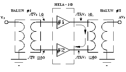
Figure 3

Figure 4-Second Harmonic Cancel
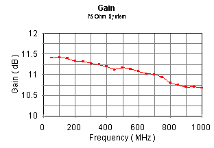
Figure 5
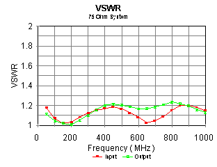
Figure 6
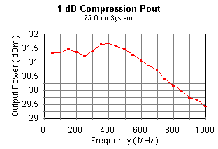
Figure 7
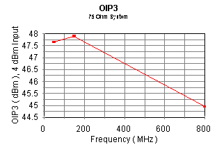
Figure 8
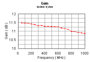
Figure 9
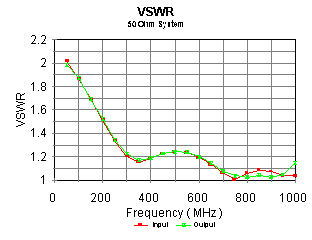
Figure 10
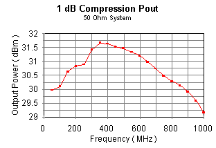
Figure 11
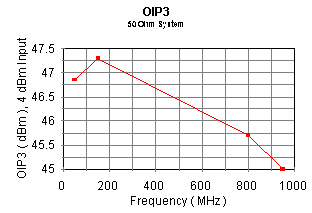
Figure 12
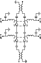
Figure 13
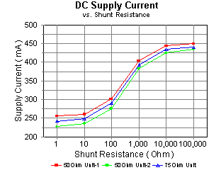
Figure 14
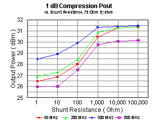
Figure 15-1
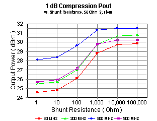
Figure 15-2

Figure 15-3
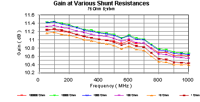
Figure 15-4
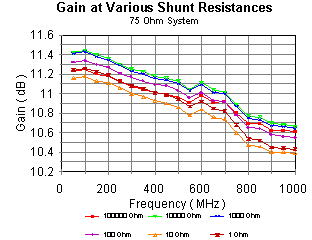
Figure 16-1
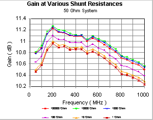
Figure 16-2
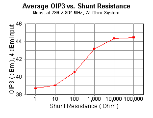
Figure 17-1
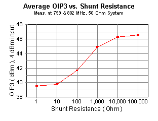
Figure 17-2

Figure 18

Figure 19-1

Figure 19-2
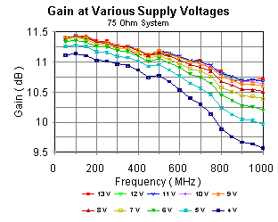
Figure 20-1
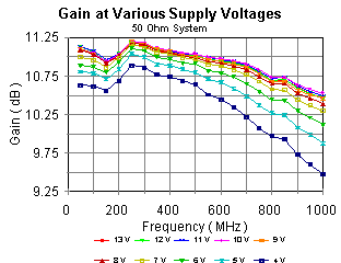
Figure 20-2
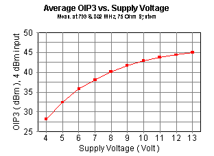
Figure 21-1

Figure 21-2