
Practical Considerations For Attaching Surface-mount Components


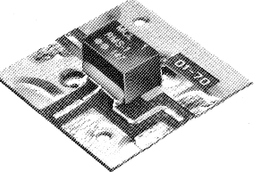
The photos included illustrate some of these components soldered to circuit boards.
What automated soldering methods can be considered for Mini-Circuits surface-mount components? There are two basic methods: reflow and wave soldering. Generally, reflow soldering can be done when (l) there are only surface mount components, or (2) these are present together with through-hole components and the latter will be soldered in a separate (wave soldering) step. The surface-mount components can be located on both the upper and lower sides of the board, when reflow is used. Wave soldering is suitable for through-hole components mounted on top of the board as well as for surface-mount components on the bottom of the board. Both ceramic and polymer-based boards can be accommodated.
reflow
Reflow requires applying a controlled amount of solder and flux to the areas where connections are to be made. A common technique is to print a pattern of solder paste on the board, and then put the components onto their places. They tend to stay in position because of the stickiness of the paste. Optionally, components can be held with chip-bonding epoxy. When heat is applied, it must produce a time-temperature profile suitable for accomplishing several process steps as illustrated in Figure l.

Fig.1 Solder Reflow Phases
First, solvent evaporation is done at temperatures up to about l00oC. Second, flux reduces metal oxides as temperature rises to the solder melting point, typically l83oC. Third, as temperature continues to rise, the solder particles in the paste melt and wetting and wicking in the joint area begin. In the next step when temperature reaches a peak around 215o, surface tension shapes the fillet of fully molten solder. It takes only a few seconds for proper solder wetting at that temperature. The length of time that the work is actually above 200o is usually limited to one or two minutes to avoid damage. Many plastic encapsulated components can withstand several minutes of solder-melt temperature when re-flowed. Even at the higher temperature experienced in wave soldering (see below) such components tend to withstand several seconds immersion in molten solder.
There are several techniques for applying the heat needed for re-flow. Two of the most common are infrared and vapor phase. Infrared heat sources operate at very high temperature and are placed at the inner walls of the chamber, not in contact with the work. The actual temperature of the work is strongly affected by its mass, geometry and composition, as well as bel speed. Organic materials such as epoxy-based boards tend to absorb the IR radiation and conduct the heat to metal parts which, by themselves, would tend to reflect the IR away. On the other hand, in the vapor-phase soldering process the vapor surrounding the work is maintained at the optimum solder-wetting temperature. This is accomplished by boiling an inert liquid in a tank. The boiling point is approximately 215oC. When the work is held in the vapor just above the liquid, the heat at that temperature is transferred to all surfaces quite uniformly.
Figures 2 and 3 illustrate profiles obtained with both re-flow processes. Separately controlled
heating zones in an IR oven provide an opportunity to shape the profile more optimally than is
typical of the vapor phase process. However, the infrared method may require more careful setup
to avoid undesired nonuniformity of heating.
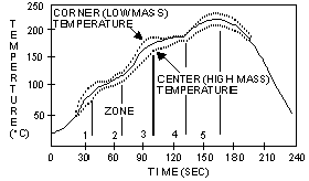
Fig. 2 Typical Five-Zone Infrared Profile.

Fig. 3 Typical Vapor Phase Profile
wave soldering
This method applied molten solder to the bottom side of a circuit board after a preheating sequence, with cool-down following the soldering. There are variations to the method, mainly characterized by the shape of the solder wave; the choice among them is influenced by the type of assembly and the components being mounted. Solder temperature, typically 260o C, is higher then the peak temperatures used in the re-flow method. The temperature profile experienced by the board and components increases during preheat to about 150o at a rate similar to re-flow, but then rises rapidly when the solder wave impinges.
Components housed in molded plastic cases may be better suited to re-flow soldering because of the possibility of micro cracks developing at the leads if they are wave soldered. Resistance to this defect is enhanced when moisture is baked out of the plastic material before soldering by either method; 24 hours at 125o C is usually effective.
some pointers
Among the considerations for successful attachment of surface-mount components are:
Leads on a component should all be in the same plane. More departure from coplanarity can be tolerated in the reflow method than in wave soldering because in reflow the surface tension in the molten solder tends to bridge small gaps and ensure an acceptable fillet. In wave soldering, special techniques are used to counteract the tendency of surface tension to deposit excess solder and cause undesired bridging between metallization areas. Even so, better coplanarity may be required when wave soldering to ensure good joints.
Wetting, or the ability of solder to adhere to the entire joint surfaces uniformly, is enhanced when clean surfaces on the component leads and circuit board are provided. If the quality of initially suitable surface finishes is preserved by proper handling and storage, the flux applied in the soldering operation should suffice to remove any metallic oxides. Compatibility of the solder includes closeness of its melting point with that of the metallization finishes, and the minimization of materials such as gold which promote the formation of brittle inter-metallic compounds with tin-lead solder. The amount of solder to be deposited depends upon joint geometry, but once determined the deposition can be controlled to a few thousandths of an inch by using pre forms or printing the solder pattern.
Concern about internal heating of components during soldering becomes greater when the size or complexity of individual components increases, or where assembly contain a mix of large and small components. In the latter case the heating rates can be disparate, or a large component may mask a small one from the source of heat. Careful study an experimentation may be needed to optimize the process. Measurement of air temperature in the processing chamber, even at several points, may not be sufficient with infrared heating. Monitoring with a surface temperature profiler can ensure that small components are not being overheated.
While high accuracy is needed for component placement on a circuit board, this requirement is eased somewhat the case of re-flow because surface tension in the molten solder has a self-centering action. This assumes that a proper metallized footprint has been provided. Correct orientation of components requires assurance that when they are supplied in tape-and-reel, all have been inserted into the tape in a constant and known orientation. Also, the tape cavity dimensions must ensure that the orientation is maintained. Especially when component placement is done manually, a clear orientation index is necessary on each component. The following considerations tend to keep the components, once placed, from becoming dislodged before the solder solidifies: When all surface-mount components are on top of the board, the stickiness of solder paste and then the surface tension of molten solder usually suffice. Components on the bottom of the board may need pre-attachment with an adhesive such as epoxy. Caution is then necessary to prevent low-viscosity constituents of the adhesive from spreading onto the metallization areas ("creep"), which could inhibit solder wetting.
automated soldering of Mini-Circuits surface-mount components
Of course, the surface-mount models listed at the beginning of the article can also be mounted by hand-soldering techniques. But, pertinent to the advantage afforded by automated assembly is that most can be soldered in their standard configurations, or require simple modification to their internal connection method or omission of a plastic enclosure, depending upon the particular temperature profile specified for a customer's application.
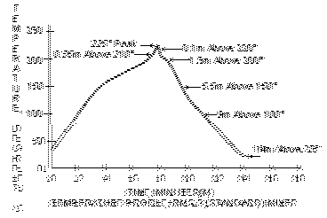
Fig. 4 Temperature Profile, RMS-2 Mixer
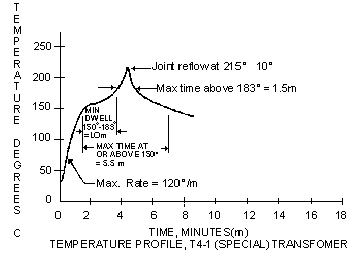
Fig. 5 Temperature Profile, T4-1 Transformer

Fig. 6 Temperature Profile, Ceramic-Base Transformer
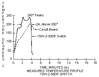
Fig. 7 Temperature Profile, YSW-2-50DR Switch
Mixer model RMS-2 meets the temperature profile shown in Figure 4 in its standard configuration. Transformer model T4-1 meets the profile in Figure 5 when a solder having 260oC solidus is used for its internal connections. A special transformer model designated TC, having a smaller version of case style TT100, has a ceramic base and no lid. It accepts the temperature profile shown in Figure 6. All three of these profiles were set by customer's specifications. As a final example, GaAs switches with drivers, in plastic case style KKK155 are designed to withstand a reflow heating and cooling cycle lasting 4 minutes, in which the component itself exceeds 200oC for 2 minutes. Figure 7 shows actual temperatures measured on a switch and on the circuit board to which it is being mounted, using an infrared reflow machine having four zones and seven source panels in a 72-inch overall length. The same GaAs switches in metal-ceramic case style AG191 will withstand a peak case temperature up to 275oC.
Last Updated: 12/17/1999