

Although I have written a piece about making PCBs using a variety of methods, I have received E-Mail asking for an explanation regarding making PCBs using photographic means. My previous article is more geared towards making 1-off prototypes than to quantity production of PCBs. It has also been pointed out that one MUST buy an expensive light-boxe to make PCBs effectively - WRONG! What I therefore propose is to make a couple of PCBs and photograph each stage of production. Please note that this method is only one method that I use. There are many other methods of ruining copper-clad boards.


Copper clad board may be bought ready coated with a photo-resist - a practice i wholheartedly reccommend. If you intend to use this then skip this section and go straight to Making the artwork.
The copper surface of the board must be sprayed with a photo-sensitive resist and cured before it is used. The coating must be applied evenly and without any dust particles or you do not stand any chance of making the PCB. I use a commercial sand-block (available from Maplins in the UK) to scrub the surface and remove all traces of oxides, tarnish, grease and other rubbish. VIM is a good proprietry household cleaner for cleaning the copper surface of PCBs, but don't dont let the wife catch you. Wash your hands thoroughly before this and again every time you are to handle the board before etching. You can make a lovely copper fingerprint of yourself by pressing your thumb on a bit of copper then etching!
 Cleaning the board
Next, wash the board under running warm water with a little soap and a nail-brush. Rinse the board well, shake it dry and blot away any remaining blobs of water that are on the surface with a bit of toilet paper (I also use the toilet for homebrew, as well as the kitchen!). Leave the board in a warm place for 30 minutes or so to become properly dry. Now close curtains / blinds and switch OFF any flourescent lighting. Use only tungsten lamps from now onwards and until the board is etched.
Now it is time to Hoover out the shack with all the doors and windows closed. Seriously! I am not kidding, any traces of dust for the next stage will cause you to waste the expensive spray laquer we use. I ALWAYS Hoover the workshop, then I Hoover the inside of an old light-tight shoebox, paying attention to all the carboard seams and corners, even the lid. By this time the washed board should be completely dry. Lay the board inside the shoebox with the copper side up then continue with the hoover to make sure the board is free from dust.
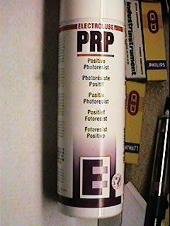 Photo Resist
There are many different types of photo resist available to the
hobbyist. here are a couple that I have used with some success:
| Product | Properties |
|---|---|
| Electrolube PRP 200 |
|
| Positive 20 |
|
| Think & Tinker Ltd
(click on the link) |
|
Until quite recently I decided upon the Electrolube PRP photoresist spray as shown above. This gave a blue laquer which becomes brown when exposed but now it is the green product. The green sprays are almost unuseable for any serious work. Seek the blue/brown and if you find one then please inform me! I have recently changed to precoated boards.
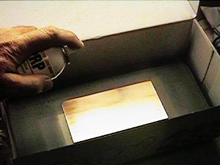 Spraying in a shoe box
Spray the PCB using even strokes, about 15cm from the board, along the length of the board, until it is COMPLETELY and EVENLY covered with the MINIMUM of resist spray possible. You will know what I mean when you try it. Put the lid on the box as soon as the board is coated, but slow enough not to create a draught. I always leave the Hoover running and hold the nozzle above the box whilst I am spraying. Now leave the box horozontal and in a warm place for a MINIMUM of 24 hours. Do NOT be tempted to peek at the board for at least an hour or you could allow dust to enter the box and contaminate the sticky laquer surface. If you need the board quickly then pop it in the oven at 50�C for 15 minutes.
OPEN DOORS AND WINDOWS TO VENTILLATE THE ROOM AS SOON AS POSSIBLE.
The propellant is toxic if inhaled so you need to do the spraying as quickly as possible. I can usually spray, close the shoebox and open the window during one breath. One word of warning: These fumes are dangerous and absolutely NO fun at all (they make you vomit!).
ERRORS

I use EASY-PC on the computer and plot the file using a Hewlet Packard plotter, but I often use a BMP image created with PC-PAINTBRUSH and send this to a laser printer. Alternatively you can often get away with feeding Overhead Projector Film into the photocopier. The image should have black areas that you cannot see through at all and clear areas without any smudges on them. You can plot/print onto ordinary typing paper but the exposure time will need to be doubled.
 My old plotter
The artwork should be printed so that the tracks are a mirror image of what you want to see on the PCB - writing should be backwards. When you lay the artwork on the board so that you see the image the correct way round then the ink (or toner) must be in direct contact with the board and you are looking through the artwork.
ERRORS

If you have more money than me then you will expose for a few minutes in a UV light-box, but us radio amateurs don't need to go to that expense. I make a contact light-frame using a bit of glass with masking tape around the edges for safety. I also cut a bit of chip-board to the same size as the glass so that I can hold the two together with a couple of elastic bands. The board and artwork are sandwiched between these so that light passes through the glass, the artwork and onto the coated copper-clad board. When you load the board and artwork into the frame, switch OFF all flourescent lamps and prevent daylight from entering the workshop. Oh, yes! Don't forget to clean the glass.
 Exposing frame
Stand this horizontally under a 40-watt DAYLIGHT flourescent lamp, about 10cm - 15cm away from the tube. Leave it for about 90 minutes. You can arrange it so that the lamp is directly over one side of the frame, then 45 minutes later rotate the frame. This will give you an even exposure, no-matter how big your PCB is. For very small PCBs it is not worth bothering about. If the artwork is good then exposure may be varied from 50% to 500% and still get a good board.
The new (green) Electrolube spray needs UV-light with a wavelength shorter than 400nm. You can knock up a cheap box and run it from 12 volts. See my INDEX page and look for USEFUL CIRCUITS.
After exposure the board must be removed from the frame so that it is not in contact with the artwork, even if you are not going to develop it for a few days. If you do not take this precaution then the photo-resist is likely to become 'burnt' in a manner that will not show up until you develop the board. The symptom is the wanted laquer dissapear before the wanted laquer. Allways store the board in complete darkness until you are ready to develop it.
ERRORS

I always keep a stock of concentrated alkaline solution made up by dissolving Caustic Soda in water. My recipe is one third of a bottle of caustic soda powder then fill the bottle up with clean water. You should always have some undisolved soda in the bottom. I also use plastic acid resistant bottles that are used to supply alcohol adatives for motor vehicles in garages. Add 2.5ml of concentrate to 100ml of water at 20�C.
SPILLAGE OF CAUSTIC SODA CAN CAUSE SERIOUS BURNS AND DAMAGE TO SKIN AND EYES. CAUSTIC SODA ALSO DISSOLVES ALUMINIUM SUCH AS COOKING UTENSILS, SINKS etc, GIVIING OFF HYDROGEN; AN EXPLOSIVE GAS.
I normally draw a sink full of cold water, and stand in it the plastic bottle containing the dry caustic soda. I then add the water slowly keeping myself clear of the top of the bottle. When the bottle is full, I put on the screw top and lay the bottle in the sink of water for about 30 minutes until almost all the soda has dissolved. If the soda should leak out of the bottle then it will be diluted with the water inthe sink. The concentrated solution should be made up at least 24 hours before needed for use, then shaken again one hour before use.
Make up a working strength solution of soda by adding about 5ml of concentrate to 200ml of 20�C water. Close windows, curtains and switch OFF all flourescent lamps. Put the exposed board in a plastic bowl and add the diluted developer. The board should not show any signs of activity for at least 30 seconds, other than a slight intensification of the barely visible PCB image on the resist. If the image shows up within a couple of seconds then the developer is far too strong and the board is ruined.
When the board is fully developed all the unwanted copper will become bare and the wanted copper tracks will still remain covered with resist. GENTLE finger pressure rubbed over the board will assist the removal of the unwanted resist as well as clearing out holes, text and other detail. Wash your hands imediately after this. The soda should be so weak that it will do no harm, but if allowed to evaporate then it could become a problem.
 Developing
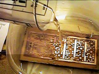
When the development is complete it is time to remove the board from the developer and wash it thoroughly under running water to remove all traces of developer.
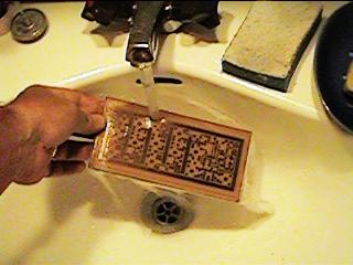 Washing
Allow the board to dry and closely inspect the board for any punctures to the resist coating. This can occur with small particles of dust during the board spraying and drying process. If the resist coating is scratched then copper will also become exposed. When this occurs I usually stick small squares of sticky tape over them before etching.
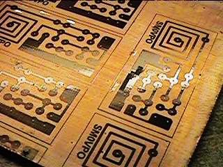 Patching damaged resist
Specks occuring in areas when copper is unwanted may be removed by scraping with a stanley knife or scalpel blade. I stick adhesive tape to the exposure frame glass so that I can easily cut out and handle small shaped bits for 'patching up' defects in the developed board.
ERRORS

There are two developers you can use, Ferric Chloride and Hydrochloric Acid/Hydrogen-peroxide. I hate ferric chloride! Actually I don't but my wife hates it and all the stains that come with it! You should see our kitchen sink! Anyway, I will describe them both for you.
| Hydrochloric (very clean) |
|
| Ferric Chloride |
|
If using the Hydrochloric etchant then just drop the board in the etchant until it is finished. If you insist on using the ferric Chloride (yeuck!!) then stick one or two strips of sticky tape to the back of the board to form one or two handles so that you can pick up the board without putting your fingers in the etchant. Lay the board on the surface of the etching solution so that it floats with the COPPER SIDE DOWN.
 Etching
Remove the board after a few seconds to inspect the surface of the copper. All the exposed copper should turn a deep "shitty brown" colour. Specks of unwanted resist or even bubbles will leave copper spots where it should not be. Remove bubbles by gently stroking the board with a paper tissue wetted with etchant. If there are specks of resist then wash and dry the board then scrape the resist of before trying again.
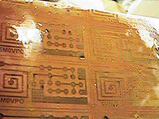 Inspecting
Notice that there is a bubble in the center of this picture (amongst all the others). This bubble has prevented the exposed copper from becomming a shitty-brown colour. The bubble must be removed with a wet tissue (I always use my finger but I cannot tell you to do that!).
If making a single sided PCB then you only have one side of copper to worry about. During etching you will normally see the PCB tracks begin to appear through the board.
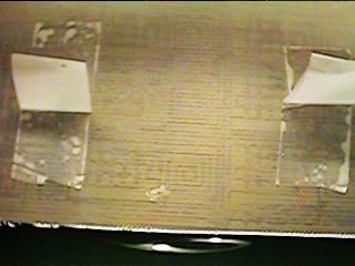 Image shows through
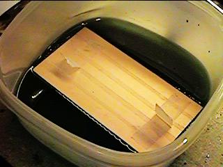 Masked double-sided PCB
Etching may be speeded up by warming the solution or adding a little salt to it. Do not use a metal vessel for etching as the etchant will attack most metals. Etching may be done during full daylight or with UV present; no harm will come to the board at this stage.
 Etched PCB
ERRORS

The laquer (photo-resist) on the copper tracks may be used as a protective cover to prevent oxidisation of the copper during storage and also gives a little mechanical protection during drilling / handling. Ialways leave the resist on the PCBs until the PCB is drilled and needed for use.
Drilling should always be done with a high-speed drill and very little force should be applied to the drill to press it through the board. Do ing so would cause the drill bit to become blunt prematurely, especially if drilling fibre-glass PCBs. It will also cause a rough edge to the board where the drill bit comes through the board. Use good sharp drill bits. Use a stable drill instrument.
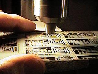 Drilling the PCB
There are many hand-held modelers drills on the market in the US$20 region, but for about US$50 you can buy a decent 'drill press' (pillar drill / upright drill / b�nkbormaskin) which has the advantage of not snapping drill bits. 0.7mm drill bits cost me over US$2 so a saving of only 25 drill bits paid for my drill press. For general PCB work I use 1mm drill bits because they are both heaper and easier to mount components.
 My drill press
The artwork must be so designed that the pads are bigger than the holes that are to be drilled in them. The artwork should also leave a 0.5mm hole in the center of each pad to guide the drill bit when the board is drilled. A high speed drill can throw fine particles which can damage eyes. Always use some form of protection, whether it be spectacles / goggles or a protective shield attached to the drilling machine. The work should also be well illuminated to help you drill the holes inthe correct places.
ERRORS

I always leave the photo-resist laquer on the board until the last minute. Remove the resist with acetone or alcohol. I use spirit of the type you get cheap to mix with petrol (benzine) at the garage. Wash and dry the board before use.
 Removing laquer
I hope that I have given you some benefit of my experience of making PCBs using the photo-etch technique. Remember that there are many other ways to make PCBs and this is not the ultimate. Just keep your eyes open in local magazines, the Internet and technical books. You may want to see my previous article on making PCBs. Photo-etch is briefly discussed, along with several other methods for making 1-off PCBs for prototypes etc.

I get loads of E-Mail regarding making PCBs so here are a couple of questions and answers.
When I put the board in the developer everything dissapears. What am I doing wrong?
There could be several reasons, the most common are (in order of likelyhood):
The image did not develop properly. I made the developer a little
stronger and it all dissapeared after 20 minutes?
Again, there could be more than one reason:
The image seemed to develop Ok but some of the copper is not even touched by the etchant?
This is because there is something between the etchant and the copper surface:
Straight edges seem bent and tracks become thinner on some parts of the board?
This is is typical of an artwork not properly pressed against the board during exposure:
The finished board looks Ok but when I hold it up to the light I see loads of little holes?
This is what happens when dust is allowed to come in contact with the board during or imediately after spraying on the photo-resist. A small speck of dust sucks up wet laquer, just like the edge of water in a glass bottle rides up the side of the bottle (cohesion). The etchant then penetrates the dust particle during etching, making the puncture hole. If the effect is bad then you could even get a 'bullseye' ring around the speck. Spray the boards when the wife is out and you can get your hands on the Hoover, as described above. If you have just the odd one or two then patch the board as described above.
The finished board looks Ok but when I hold it up to the light I see loads of thin but long slits. Some of the tracks are also broken?
Exactly the same as above, but the board was contaminated by hairs, eyelashes etc. If you have long hair then wear a 'Benny Hill' hat when spraying. Perhaps you didn't hoover the rest of the workshop before you sprayed? (naughty naughty!).
I have made the board and half of it looks Ok but the other half
did not develop?
Most of the board is perfect, especially in the middle, but near the edges it did not seem develop properly?
The board was sprayed with too much resist spray and the layer of laquer is not even. With too much spray then you will allways get a thicker layer of resist about a centimeter from each edge.
Have fun but most of all be carefull. Making PCBs can be fun but it can also be very harmful if insufficient care is exercised. The dangers of Caustic Soda, Ferric Chloride, Hydrochliric Acid and electric drills can never be sufficiently emphasised. If you kill yourself then don't complain to me. 73s de HARRY, Upplands Vasby, Sweden.