MB1504 PLL Frequency Synthesizer

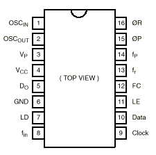
PIN-description
SERIAL INPUT PLL FREQUENCY SYNTHESIZER WITH 520MHz PRESCALER
The Fujitsu MB1504/MB1504H/MB1504L, utilizing BI-CMOS technology, is a single chip serial input PLL frequency synthesizer with pulse-swallow function.
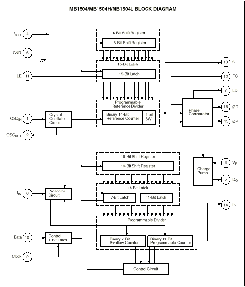
The MB1504 series contains a 520MHz two modulus prescaler that can select either 32/33 or 64/65 divide ratio; control signal generator; 16-bit shift register; 15-bit latch; programmable reference divider (binary 14-bit programmable reference counter); 1-bit switch counter; phase comparator with phase inverse function; charge pump; crystal oscillator; 19-bit shift register; 18-bit latch; and a programmable divider (binary 7-bit swallow counter and binary 11-bit programmable counter).
The MB1504 operates from a low supply voltage (3V typ) and consumes low power (30mW at 520MHz).
Block Diagram
FEATURES
 High operating frequency: fIN MAX =520MHz (VIN MIN =0.20VP-P)
 On-chip prescaler
 Low power supply voltage: 2.7V to 5.5V (3.0V typ)
 Low power supply consumption: 30mW (3.0V, 520MHz operation)
 Serial input 18-bit programmable divider consisting of:
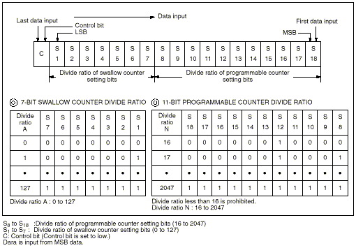
–Binary 7-bit swallow counter (Divide ratio: 0 to 127)
–Binary 11-bit programmable counter (Divide ratio: 16 to 2047)
 Serial input 15-bit programmable reference divider consisting of:
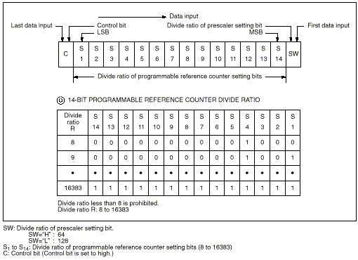
–Binary 14-bit programmable reference counter (Divide ratio: 8 to 16383)
–1-bit switch counter (SW) Sets divide ratio of prescaler
 2 types of phase detector output
–On-chip charge pump (Bipolar type)
–Output for external charge pump

Pin Name Description
1 OSCIN Crystal oscillator connection pin serving as a reference divider input pin (Oscillator circuit input pin)
2 OSCOUT Crystal oscillator connection pin (Oscillator circuit output pin)
3 VP Power supply pin for charge pump output. Connect this pin to VCC when the internal charge pump is not used.
4 VCC Power supply pin
5 DO Internal charge pump output pin
6 GND GND pin
7 LD Lock detector output pin. When locked: LD = “H”, When unlocked: LD = “L”
8 fIN Prescaler input pin. The pin must be AC-coupled for input.
9 Clock Clock input pin for 19-bit and 16-bit shift registers. The shift resistors reads data at the rise of the clock pulse.
10 Data Binary-coded serial data input pin. The last bit in the data is a control bit.
Control bit = “H”: Sends data to the 15-bit latch.
Control bit = “L”: Sends data to the 18-bit latch.
11 LE Load enable signal input pin (with pull-up resistor). When LE = “H”, the pin sends the contents of the shift register to the latch according to the control bit.
12 FC Phase comparator phase switching pin (with pull-up resistor). When FC = “L”, the pin inverts characteristics of the phase comparator. It also switches the fout pin (test pin) output between fr and fp.
13 fr Monitor pin of phase comparator input. It is the same as the programmable reference divider output.
14 fp Monitor pin of phase comparator input. It is the same as the programmable divider output.
15 øP Phase comparator output pin for external charge pump. This pin is an N channel open-drain output.
16 øR Phase comparator output pin for external charge pump. This pin is a CMOS output.


FUNCTIONAL DESCRIPTIONS
Pulse Swallow Function
For the pulse swallow function, use the following equations to select their respective setting values:
fVCO = ((P x N) + A) x fOSC / R
fVCO : Output frequency of externally connected VCO
P : Prescaler divide ratio (64 or 128)
N : Divide ratio of 11-bit programmable counter (16 to 2047)
A : Divide ratio of 7-bit swallow counter (0 to 127, A < N)
fOSC : Reference oscillation frequency
R : Divide ratio of 14-bit programmable reference counter (6 to 16383)

Serial Data Input Method
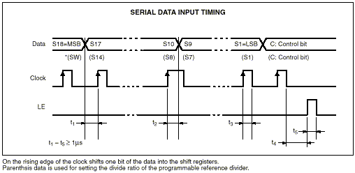
Serial data is processed using three input pins (Data, Clock, and LE pins) to control the 15-bit reference divider and the 18-bit programmable divider separately.
Input binary-coded serial data to the Data pin.
Serial data is input to the internal shift register in sequence at the rise of each clock pulse. When the load enable signal input pin has a high level (or open), the input data is transferred to the latch depending on the control bit.
Control bit = “H”: Transfer to the 15-bit latch
Control bit = “L”: Transfer to the 18-bit latch

Serial Data Input Timing

Divide Ratio of Reference Divider
The reference divider consists of a 16-bit shift register, a 15-bit latch, and a 14-bit reference counter. Serial data is made up of the following 16 bits:
Serial Data to Reference Divider

Divide Ratio of Programmable Divider
The programmable divider consists of a 19-bit shift register, an 18-bit latch, 7-bit swallow counter, and an 11-bit programmable counter. Serial data is made up of the following 19 bits:
Serial Data to Programmable Divider