
|
The Audio Pages |
| Elliott Sound Products | Project 76 |
Opamp Based Power Amplifier
Rohit Balkishan
This is a contributed project from Rohit Balkishan, who has built it, and thought that it would make a nice simple project for others. This is a good experimental project, will be cheap to make, and you will learn from it.
This project has recently been updated (09 Aug 2001), it is more reliable and operates the opamps from a regulated supply.
The amplifier is based on the commonly used class-AB complementary power amplifier with compound pair output transistors. The system uses a TL074 quad opamp to drive the output transistors. As can be seen from figure 1, A2 is used to set the voltage gain of the amplifier. Assuming the voltage gain of a common collector stage to be unity, the overall voltage gain of the amplifier is equal to (R4 / R3) + 1, i.e. the gain of a non-inverting OP-AMP (16 or 24dB, in this case). Since the output transistors are within the feedback loop of A2, A2 also acts to linearise the input characteristic of the complementary pair Q1/Q2 & Q3/Q4. This allows for greater mismatch between the NPN-PNP transistors.
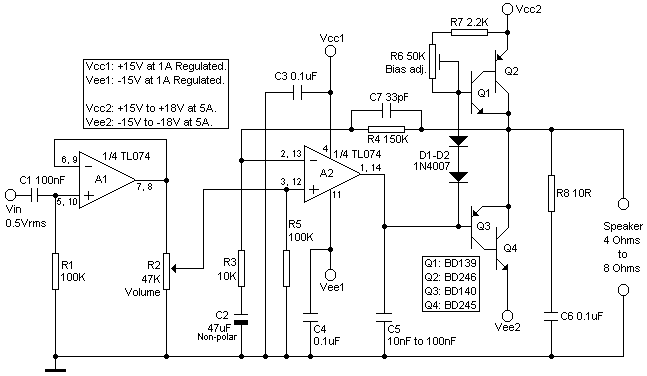
Figure 1 - Power Amplifier
Schematic
A supply of up to +/-22V is OK for the power transistors, and allows the same supply to power the regulators. Lower voltages (as shown) will be insufficient to provide the regulators with sufficient reserve input voltage. (ESP)The biasing to Q1 & Q3 is provided by R6, R7 & diodes D1 & D2. This arrangement biases the transistors just above cut-off and reduces crossover distortion. R6 must be adjusted to the highest value which eliminates crossover distortion. Ideally D1 & D2 should be mounted so they are in contact with the driver transistors - not the main heatsink.
To adjust R6 without an oscilloscope, start with R6 set to maximum, set the volume control R2 to get the minimum audible output with a suitable input source (such as a CD player which gives 0.65Vrms at line out), and listen for any "crackle" in the sound, especially that which seems to be riding on low frequency sounds. If a "crackle" is heard then reduce the value of R6 in very small steps, until the crackle (crossover distortion) becomes inaudible (it can't be eliminated, I feel).
As the output of opamp A2 is being pulled up by the biasing circuit, capacitor C5 must be connected between the output of A2 and ground to prevent the circuit from breaking into oscillations. The value of C5 is not critical, any value between 22nF to 100nF will do. The opamp A1 is a simple buffer which isolates the input circuit from the power stage. C1 & R1 are used to set the lower 3db frequency to around 15Hz, and to obtain an input impedance of about 100K. The upper 3db frequency is determined by R4 & C7, which in this case is approximately 30KHz. The schematic shows only one channel of the stereo amplifier. The amplifier can be used to drive speakers with impedance ranging from 3 Ohms to 8 Ohms, higher impedance speakers could be used but the power output will be substantially less.
The voltage gain of the amplifier can be increased by increasing R4 or decreasing R3, as long as the output swing is kept less than or equal to 3 Volts below the supply rails. This is due to the fact that the maximum output voltage of an opamp is always 2-3 Volts less than the supply rails, before it clips.
The voltage gain of the amplifier is 16 or 24db (R3 = 10K & R4 = 150K). Also, note that the values of R3 & R4 are not critical as far as their absolute values are concerned, what is critical, however, is their ratio (Av = 1 + R4 / R3). Choose C7 to give an upper 3db frequency of about 30KHz - 50KHz. I haven't measured the actual power output of the prototype that I have built as yet, but I have put it to normal use, nevertheless.
Any transistors which satisfy the following criteria
can be used:
Q1/Q3: Vmax >= 40V, Imax >= 1A, Pmax > = 5W, hfe
> = 25, Ft > = 50KHz
Q2/Q4: Vmax >= 40V, Imax >= 5A, Pmax > = 40W, hfe
> = 20, Ft > = 50KHz
The transistors shown are somewhat costly due to the fact that they are HF transistors with Ft = 4MHz and also have higher voltage/power ratings than required, that's because originally I had intended to build an amplifier which can drive +/-33Volts into a 4 Ohms load, but due to the non-availability of the LM3580 quad opamp, I went for a lower power version, but the transistors stayed. For this current design however, lower cost AF transistors can well be used.
The entire circuit along with it's power supply can be easily assembled on a general purpose veroboard. Various kinds of opamps, transistors can be used in place of those shown here to obtain a high performance system. For example opamps like OP445 (high speed/high slew rate) LM3580 or LM3581 (high voltage) may be used in the design with increased cost and better performance, or almost any general purpose opamps can be used to get a decent working system at a low cost.
The modifications to the original circuit are ...
The transistors Q2 & Q4 can be changed to BD240/MJ2955 and BD239/2N3055 respectively. BD239/240 to be used only if the load impedance is greater than or equal to 6 Ohms. For lower impedances, either retain the shown transistors or use higher current transistors (2N3055/MJ2955 and the like). The heat sinks need not be very elaborate (except with BD239/240), since the transistors have power ratings well in excess of those required. In spite of this, a large heat sink is always better than a smaller one.
Due to reduction in the supply voltages to the Op-Amps, the max. o/p swing will now be about +/-12 V(p-p) or a power of 18W into a 4 Ohms load, or 9W into 8 Ohms. This value of power is a very modest figure and as such this amp won't be very loud. To get a system that gives appreciable power, it's better to use this amp for bi/tri-amping with active crossovers. Assuming an absolute max. power of 20 W into 4 Ohms, we can obtain 40 W (60 W) by bi-amping (tri-amping). For a stereo system, this equates to 80 W (120 W) of total power output, which is quite sufficient for home use. The amp has a fairly respectable frequency response, and the highs are extremely clear, hence it is recommended that this amp be used in a bi/tri-amplified system instead of stand-alone. For a tri-amped system (or a bi-amped system which uses only a tweeter for mid+high), a 22uF non-polar capacitor must be used in series with the o/p of the amp feeding the tweeter.
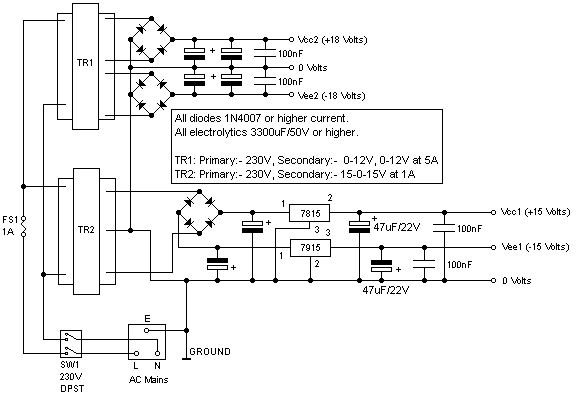
Figure 2 - Power Supply
The performance of any electronic system depends to a large extent on the power supply that it contains, i.e. on how well the supply is regulated and how well it rejects hum/ripple. Any dual power topology could have been used for this amplifier, but by far the best power supply is the good old bridge rectifier/capacitor filtered system. This type is simple to assemble, straight-forward, low-cost and can be made to have very good regulation & ripple rejection by proper choice of transformers and filter capacitors.
The above schematic contains 2 separate transformer/rectifier/filter chains. This arrangement requires that the upper transformer has output voltages that are very close to each other (of course, some variation is acceptable as long as the final DC voltages are within 0.5V to 1V of each other). The upper chain is for the power transistors (high current) and the lower one is for the op-amps (low current). The only stringent requirement here is that the upper transformer must be able to supply a current of at least 5 amperes on each half cycle of the output (this is needed for good regulation, especially when the amplifier is operated at or near maximum power).
The upper transformer rating is shown to be greater than is actually required (even 2 to 3 amps is good enough), so that this supply can be used for bi/tri-amped systems. The upper transformer can be a 12-0-12V unit with the centre tap split to obtain two 0-12V outputs. A 12-0-12V transformer would require that the diodes be rated at least double that of the present rating. Using it as a dual 0-12V unit places a somewhat lesser demand on the diodes. A better idea would be to use a 10 to 35A bridge for the upper transformer.
The capacitors must be rated at 3300uF/50V or higher (a higher value will improve ripple rejection & regulation). Due to the class AB topology of the amplifier, the amplifier is inherently immune (more or less) to bad supply regulation and hence a simple power supply such as this one is more than sufficient for this application. Care must be taken while assembling the power supply, so that the mains hum is not picked up at the input and proper insulation must be used to eliminate any risk of an electric shock. This supply can be used for both channels of a stereo system, even if they are bi/tri-amped. Bypassing the electrolytics with 100nF capacitors is not mandatory but is recommended.
Editor's Notes: The 1N4007 diodes suggested do not have a high enough current rating, and I suggest that bigger diodes be used. Diodes for this circuit should ideally be rated at a minimum of 5A continuous.See the Power Supply Design article for more details on the design of power supplies.
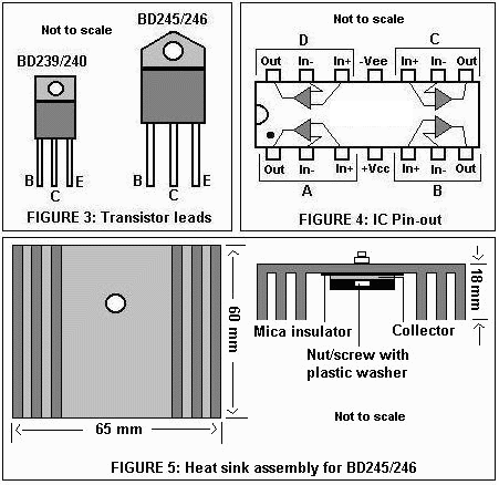
Figures 3 and 4 show the transistor leads and IC pin-out respectively. As with any power system, this amplifier also produces some heat in it's output devices and these must be provided with a proper means to dissipate the generated heat. The transistors BD245/246 must be mounted on proper heat sinks such as the one shown in figure 5. The collectors of the transistors must have a proper thermal (NOT electrical) contact with the heat sinks. A mica insulator must be sandwiched between the collector and the heat sink. Also, a plastic "through and through" washer must be inserted in the transistor & heat sink holes such that the screw used to secure the transistor to the heat sink is electrically insulated from both the collector as well as the heat sink. Use of some heatsink compound (a kind of paste) on the faces of the mica insulator improves the heat transfer from the collector to the heat sink.
That concludes the description of the entire project. I hope that the reader will find the material presented to be of some help in understanding amplifiers in particular and electronics in general. The following books/materials were used for reference:
1) Integrated Electronics by Millman & Halkias, Tata McGraw-Hill (ISBN 0-07-Y85493-9)
2) National Semiconductor Opamp data book.
| Copyright Notice. This article,
including but not limited to all text and diagrams, is the intellectual
property of Rohit Balkishan and Rod Elliott, and is Copyright |