Design Guidelines for Bipolar Transistor Audio Preamplifier Circuits
By Mike Martell
N1HFX
 
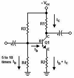
  Before attempting to design a transistor amplifier circuit, it is necessary to acquaint ourselves with some very important design equations. The most commonly used design equations are listed to the right to help us with our effort. The first few equations are derived from ohms law and you should already be familar with them. The bottom two equations deal with transistor gain and are equally important to our work. The formula for hfe refers to the ratio of collector current (Ic) to base current (Ib). For most modern transistors it is typically in the 50 to 100 range. To insure a circuit will always work properly, it is safe to assume a value of 50 for modern transistors.  
       
  At this time, we need to make some decisions about our audio preamplifier circuit. For this design example we will choose the following:
  • Vcc = 12 V
  • Ic = 5 ma
  • hfe = 50
  • Q1 = 2N3904

With all those big decisions made, we can now begin our design.


Using the one of the hfe formulas, we will now calculate the base current as follows:

Ib = Ic / hfe
Ib = .005 / 50 = .1 ma

Lets calculate R1, the collector load resistor, as follows:

R1 = 1/2Vcc / .005
R1 = 6 / .005 = 1200

Notice above that we assumed 1/2 of the supply voltage to be dropped accross R1. This is necessary to insure that the amplifier remains in the linear operating range of the transistor.

We need to determine how much voltage is to appear across the emitter resistor, R2, before we calculate its value. A good value is anywhere between 5 to 10 percent of Vcc. For this circuit we will use 1 volt which is about 8 percent of Vcc. Resistor R2 is now calculated as follows:

R2 = 1 / (Ic + Ib)
R2 = 1 / (.005 + .0001) = 196

Because the voltage across the base to emitter of a silicon transistor is always .7 volts, the voltage from the base to ground is .7 plus the 1 volt drop across R2 for a total of 1.7 volts. This 1.7 volts happens to be the voltage drop across resistor R4. In order to provide a stiff base voltage, resistor R4 should have a current of about 5 to 10 times the base current. For this example, we will assume 9 times the base current for a total of .9 ma. Resistor R4 can now be calculated as follows:

R4 = 1.7 volts / .0009 = 1889

If the voltage drop across R4 is 1.7 volts then the voltage drop across R3 must be 12 - 1.7 for a total of 10.3 volts. The current through R3 is the total of the current through R4 (.9ma) and the base current (.1ma) for a total of 1 ma. R3 can now be calculated as follows:

R3 = 10.3 / .001 = 10300

Now that we have calculated all our resistor values, we will select the nearest standard values as indicated below:


R1 = 1.2K
R2 = 180
R3 = 10K
R4 = 1.8K

The circuit at right is the result of our design efforts. 4.7uF capacitors were use for input and output coupling and slightly larger or small values could be used satisfactorily. Notice the optional 4.7uf capacitor across the emitter resistor R2. This capacitor increases the current gain to the hfe of the particular transistor used. This emitter bypass capacitor should only be used when the maximum amount of gain is desired without regard to a predictable level of gain.

 
  Remember, hfe will vary from transistor to transistor even though they have the same part number and even if they were produced by the same manufacturer. It is always better to assume an hfe that is at least 20% less than that specified by the manufacturer.

One common error that designers make is that they forget to calculate the actual power that each resistor will dissipate in a circuit. Failure to perform these calculations can sometimes result in a resistor exceeding its maximum power level and cause premature resistor failure. This is particularly important for circuits which have collector currents exceeding 40 milliamps. Fortunately, power ratings for each of our resistors in this circuit can be easily calculated as follows:

R1 = 6 Volts * .005 Amps = .03 Watts
R2 = 1 Volt * .0051 Amps = .0051 Watts
R3 = 10.3 Volts * .001 Amps = .0103 Watts
R4 = 1.7 Volts * .0009 Amps = .00153 Watts

The preceding calculations indicate that 1/4 watt, 5% resistors are adequate for this design.

Although our preceding circuit does have substantial gain, lets design a second stage to the previous circuit to further increase gain. Before we can begin our design we must make those all important design decisions again as indicated below:

Q1 = 2N3904
Vcc = 12V
Ic = 10ma
hfe = 50
Vr2 = 1V (8% of Vcc)
Ir4 = 9 times Ib

Now were ready to calculate our resistor values as follows:

R1 = 6/.010 = 600
Ib = .01/50 = .0002
R2 = 1/(Ic + Ib) = 1/(.01 + .0002) = 98
Ir4 = 9 * .0002 = .0018
R4 = (1 + .7)/.0018 = 944
R3 = (12 - 1 - .7)/(.0018 + .0002) = 10.3 / .002 = 5150

 
We will select standard resistor values as follows:

R1 = 560
R2 = 100
R3 = 5.1K
R4 = 1K

The circuit at right is the result of our design efforts. 10uF capacitors were use for output coupling and optional emitter bypass. Slightly larger or small capacitor values could also be used satisfactorily. As always, the emitter bypass capacitor should only be used when the maximum amount of gain is desired without regard to a predictable level of gain.


Now lets add the two transistor stages together to get the resulting circuit below:.

Because of the large amount of gain obtained with this circuit, we added a 10K variable resistor at the output as a gain control. This circuit will provide good results for almost any microphone preamplifer application. Incidentially, we can substitute a 2N2222A, 2N4401 or any general purpose NPN with a minimum hfe of 50 for the 2N3904 transistor used in this design example. There are many general purpose NPN transistors that can be easily used in this circuit with good results.

Perhaps a good exercise for the designer is to recalculate all of the above resistor values using a Vcc of 9 volts which will allow the use of a 9 volt battery.

Now that we got our hands wet designing these circuits, lets summarize what we've learned below:

     
  Vcc = Supply Voltage
  hfe = Absolute minimum current gain for the selected transistor
  Ic = Selected collector current
  Ib = Ic / hfe (base current)
     
  Vr1 = 1/2 Vcc
  Vr2 = 5 to 10% of Vcc
  Vr3 = Vcc - .7 - Vr2
  Vr4 = .7 + Vr2
     
  Ir4 = 5 to 10 times Ib
     
  R1 = 1/2Vcc / Ic
  R2 = Vr2 / (Ic + Ib)
  R3 = (Vcc - .7 - Vr2) / (Ir4 + Ib)
  R4 = (.7 + Vr2) / Ir4


DE N1HFX

Back to Projects Page!