
| Elliott Sound Products | Amplifier Basics - How Amps Work |
Copyright
(c) 1999 - Rod Elliott (ESP)
Page Last Updated 09 Jun
2001
The term "amplifier" has become generic, and is often thought (at least by some) to mean a power amplifier for driving loudspeakers. This is not the case (well, it is, but it is not the only case), and this article will attempt to explain some of the basics of amplification - what it means and how it is achieved. This article is not intended for the designer (although designers are more than welcome to read it if they wish), and is not meant to cover all possibilities. It is a primer, and gives fairly basic explanations (although some will no doubt dispute this) of each of the major points.
I will explain the basic amplifying elements, namely valves (vacuum tubes), bipolar transistors and FETs, all of which work towards the same end, but do it differently. This article is based on the principles of audio amplification - radio frequency (RF) amplifiers are designed differently because of the special requirements when working with high frequencies.
Not to be left out, the opamp is also featured, because although it is not a single "component" in the strict sense, it is now accepted as a building block in its own right.
This article is not intended for the complete novice (although they, too, are more than welcome), but for the intermediate electronics or audio enthusiast, who will have the most to gain from the explanations given.
I must also apologise for the size of this
file - at over 120k is is a little larger than I had originally intended.
If you have difficulties because of the size, please let me know so I can
break it down into smaller sections.
Before we continue, I must explain some of the terms that are used. Without knowledge of these, you will be unable to follow the discussion that follows.
Electrical Units
| Name | Measurement of | A.K.A. | Symbol |
| Volt | electrical "pressure" | voltage | V |
| Ampere | the flow of electrons | current | A, I |
| Watt | power | W, P | |
| Ohm | resistance to current flow | ||
| Ohm | impedance, reactance | ||
| Farad | capacitance | F, C | |
| Henry | inductance | H, L | |
| Hertz | frequency | Hz |
Note: A.K.A. means "Also Known As". Although the Greek letter omega is the symbol for Ohms, I shall use the word Ohm or the letter "R" to denote Ohms. Any resistance of greater than 1,000 Ohms will be shown as (for example) 1k5, meaning 1,500 Ohms, or 1M for 1,000,000 Ohms. The second symbol shown in the table is that commonly used in a formula.
When it comes to Volts and Amperes (Amps), we have alternating current and direct current (AC and DC respectively). The power from a wall outlet is AC, as is the output from a CD or tape machine. The mains from the wall outlet is at a high voltage and is capable of high current, and is used to power the amplifying circuits. The signal from your audio source is at a low voltage and can supply only a small current, and must be amplified so that it can drive a loudspeaker.
Impedance
A derived unit of resistance, capacitance
and inductance in combination is called impedance, although it is not a
requirement that all three be included. Impedance is also measured
in Ohms, but is a very complex figure, and often fails completely to give
you any useful information. The impedance of a speaker is a case
in point. Although the brochure may state that a speaker has an impedance
of 8 Ohms, in reality it will vary depending on frequency, the type of
enclosure, and even nearby walls or furnishings.
Units
In all areas of electronics, there are
smaller and larger amounts of many things that would be very inconvenient
to have to write in full. For example, a capacitor might have a value
of 0.000001F or a resistor a value of 150,000 Ohms. Because of this,
there are conventional units that are applied to make our lives easier
(well, once we are used to using them, anyway). It is much easier
to say 1uF or 150k (the same as above, but using standard units).
These units are described below.
Conventional Metric Units
| Symbol | Name | Multiplication |
| p | pico | 1 x 10-12 |
| n | nano | 1 x 10⁻⁹ |
| micro | 1 x 10⁻⁶ | |
| m | milli | 1 x 10⁻³ |
| k | kilo | 1 x 10³ |
| M | Mega | 1 x 10⁶ |
| G | Giga | 1 x 10⁹ |
| T | Tera | 1 x 10¹² |
Although commonly written as the letter "u", the symbol for micro is actually the Greek letter mu as shown. Because this would require the continuing use of a small graphic, I shall use the letter "u".
In audio, Giga and Tera are not commonly
found (not at all so far - except for specifying the input impedance of
some opamps!). There are also others (such as femto - 1x10-15)
that are extremely rare and were not included. Of the standard electrical
units, only the Farad is so large that the defacto standard is the microFarad
(uF). Most of the others are reasonably sensible in their basic form.
The term "amplify" basically means to make stronger. The strength of a signal (in terms of voltage) is referred to as amplitude, but there is no equivalent for current (curritude?, nah, sounds silly). This in itself is confusing, because although "amplitude" refers to voltage, it contains the word "amp", as in ampere. Maybe we should introduce "voltitude" - No? Just live with it.
To understand how any amplifier works, you need to understand the two major types of amplification, and a third "derived" type:
In the case of a current amplifier, an input current of 10mA (0.01A) might be amplified to give an output of 1A. Again, this is a gain of 100, and is the current gain of the amplifier.
If we now combine the two amplifiers, then
calculate the input power and the output power, we will measure the power
gain:
P = V x I (where
I = current, note that the symbol changes in a formula)
The input and output power can now be calculated:
Pin = 0.01 x 0.01 (0.01V
and 0.01A, or 10mV and 10mA)
Pin = 100uW
Pout = 1 x 1 (1V
and 1A)
Pout = 1W
The power gain is therefore 10,000, which is the voltage gain multiplied by the current gain. Somewhat surprisingly perhaps, we are not interested in power gain with audio amplifiers. There are good reasons for this, as shall be explained in the remainder of this page. Having said this, in reality all amplifiers are power amplifiers, since a voltage cannot exist without power unless the impedance is infinite. This is never achieved, so some power is always present, but it is convenient to classify amplifiers as above, and no harm is done by the small error of terminology.
Input Impedance
Amplifiers will be quoted as having a
specific input impedance. This only tells us the sort of load it
will place on preceding equipment, such as a preamplifier. It is
neither practical nor useful to match the impedance of a preamp to a power
amp, or a power amp to a speaker. This will be discussed in more
detail later in this article.
The load is that resistance or impedance placed on the output of an amplifier. In the case of a power amplifier, the load is most commonly a loudspeaker. Any load will require that the source (the preceding amplifier) is capable of providing it with sufficient voltage and current to be able to perform its task. In the case of a speaker, the power amplifier must be capable of providing a voltage and current sufficient to cause the speaker cone(s) to move. This movement is converted to sound by the speaker.
Even though an amplifier might be able to make the voltage great enough to drive a speaker cone, it will be unable to do so if it cannot provide enough current. This has nothing to do with its output impedance. An amplifier can have a very low output impedance, but only be capable of a small current (an operational amplifier, or opamp is a case in point). This is a very important point, and needs to be fully understood before you will be able to fully appreciate the complexity of the amplification process.
Output Impedance
The output impedance of an amplifier is
a measure of the impedance or resistance "looking" back into the amplifier.
It has nothing to do with the actual loading that may be placed at the
output.
For example, an amplifier has an output impedance of 10 Ohms. This is verified by placing a load of 10 Ohms across the output, and the voltage can be seen to decrease by 1/2. However, unless this amplifier is capable of substantial output current, we might have to make this measurement at a very low output voltage indeed, or the amplifier will be unable to drive the load.
Another amplifier might have an output impedance of 100 Ohms, but be capable of driving 10A into the load. Impedance and current are completely separate, and must not be seen to be in any way equivalent. Both of these possibilities will be demonstrated later in this article.
Feedback
Feedback is a term that creates more and
bloodier battles between audio enthusiasts than almost any other.
Without it, we would not have the levels of performance we enjoy today,
and many amplifier types would be unlistenable without it.
Feedback in its broadest sense means that a certain amount of the output signal is "fed back" into the input. An amplifier - or an element of an amplifying device - is presented with the input signal, and compares it to a "small scale replica" of the output signal. If there is any difference, the amp corrects this, and ideally ensures that the output is an exact replica of the input, but with a greater amplitude. Feedback may be as a voltage or current, and has a similar effect in either case.
In many designs, one part of the complete amplifier circuit (usually the input stage) acts as an error amplifier, and supplies exactly the right amount of signal to the rest of the amp to ensure that there is no difference between the input and output signals, other than amplitude. This is (of course) an ideal state, and is never achieved in practice. There will always be some difference, however slight.
Signal Inversion
When used as voltage amplifiers, all the
standard active devices invert the signal. This means that if a positive
signal goes in, it emerges as a larger - but now negative - signal.
This does not actually matter for the most part, but it is convenient (and
conventional) to try to make amplifiers non-inverting. To achieve
this, two stages must be used (or a transformer) to make the phase of the
amplified signal the same as the input signal.
The exact mechanism as to how and why this happens will be explained as we go along.
Design Phase
The design phase of an amplifier is not
remarkably different, regardless of the type of components used in the
design itself. There is a sequence that will be used most of the
time to finalise the design, and this will (or should) follow a pattern.
For the sake of simplicity, if bipolar
output transistors have a gain of 20 at the maximum current into the load,
the drivers must be able to supply enough base current to allow this.
If the maximum current is 4A, then the drivers must be able to supply 200mA
of base current to the output devices.
Again, using the bipolar example from above,
the maximum base current for the output transistors was 200mA. If
the drivers have a minimum specified gain of 50, then their base current
will be
200 / 50 = 4mA.
Since the Class-A driver must operate
in Class-A (what a surprise), it will need to operate with a current of
1.5 to 5 times the expected maximum driver current, to ensure that it never
turns off. The same applies with a MOSFET amp that will expect (for
example) a maximum gate capacitance charge (or discharge) current of 4mA
at the highest amplitudes and frequencies.
This is not normally an issue with valve
amps, as the early stages of the amp are not loaded with any significant
impedance. No further determinations are needed (other than the normal
loading effects of valve stages in general).
Information added 09 Jun
2001
For the purposes of this article, there are three different types of amplifying devices, and each will be discussed in turn. Each has its strengths and weaknesses, but all have one common failing - they are not perfect.
A perfect amplifier or other device (known generally as "ideal") will perform its task within certain set limits, without adding or subtracting anything from the original signal. No ideal amplifying device exists, and as a result, no ideal amplifier exists, since all must be built with real-life (non-ideal) devices.
The amplifying devices currently available are:
All of these devices are reliant on other non-amplifying ("support") components, commonly known as passive components. The passive devices are resistors, capacitors and inductors, and without these, we would be unable to build amplifiers at all.
All the devices we use for amplification have a variable current output, and it is only the way that they are used that allows us to create a voltage amplifier. Valves and FETs are voltage controlled devices, meaning that the output current is determined by a voltage, and no current is drawn from the signal source (in theory). Bipolar transistors are current controlled, so the output current is determined by the input current. This means that no voltage is required from the signal source, only current. Again, this is "in theory", and it is not realisable in practice.
Only by using the support components can
we convert the current output of any of these amplifying devices into a
voltage. The most commonly used for this purpose is a resistor.
All active devices have certain parameters in common (although they will have different naming conventions depending on the device). Essentially these are
With most semiconductors, in many cases
it will not be possible to operate them at anywhere near the maximum power
dissipation, because thermal resistance is such that the heat simply cannot
be removed from the junction and into the heatsink fast enough. In
these cases, it might be necessary to use multiple devices to achieve the
performance that can (theoretically) be obtained from a single component.
This is very common in audio amplifiers.
There are some things that you just can't get away from, and maths is one of them. (Sorry.) I will only include the essentials here, but will describe any others that are needed as we go. I am not about to give a lesson in algebra, but the best reason for ever doing the subject is to learn how to transpose electronics formulae ! Transposition is up to you (unless I am forced to do it for a calculation here or there).
Ohm's Law
The first of these is Ohm's Law, which
states that a voltage of 1V across a resistance of 1 Ohm will cause a current
of 1 Amp to flow. The formula is
R = V / I (where
R = resistance in Ohms, V = Voltage in Volts, and I = current in Amps)
Like all such formulae, this can be transposed
(oops, I said I wasn't going to do this, didn't I),
V = R * I (
*
means multiplied by), and
I = V / R
Reactance
Then there is the impedance (reactance)
of a capacitor, which varies inversely with frequency (as frequency is
increased, the reactance falls and vice versa).
Xc = 1 / (2 * ![]() * f * C)
* f * C)
where Xc is capacitive reactance in Ohms, ![]() (pi) is 3.14159, f is frequency in Hz, and C is capacitance in Farads.
(pi) is 3.14159, f is frequency in Hz, and C is capacitance in Farads.
Inductive reactance, being the reactance
of an inductor. This is proportional to frequency.
Xl = 2 * ![]() *
f * L
*
f * L
where Xl is inductive reactance in Ohms, and L is inductance in Henrys (others as above).
Frequency
There are many different calculations
for this, depending on the combination of components. The -3dB frequency
for resistance and capacitance (the most common in amplifier design) is
determined by
fo = 1 / (2 * ![]() * R * C) where
fo is the -3dB frequency
* R * C) where
fo is the -3dB frequency
When resistance and inductance are combined,
the formula is
fo = R / (2 * ![]() * L)
* L)
(The above formula was incorrect as shown before - thanks to a reader for pointing this out)
Power
Power is a measure of work, which can
be either physical work (moving a speaker cone) or (much more commonly
in audio), thermal work - heat. Power in any form where voltage,
current and resistance are present can be calculated by a number of means:
P = V * I
P = V2 /
R
P = I2 *
R
where P is power in watts, V is voltage in Volts, and I is current in Amps.
Decibels (dB)
It has been known for a very long time
that human ears cannot resolve very small differences in sound pressure.
Originally, it was determined that the smallest variation that is audible
is 1dB - 1 decibel, or 1/10 of 1 Bel. It seems fairly commonly accepted
that the actual limit is about 0.5dB, but it is not uncommon to hear that
some people can (or genuinely believe they can) resolve much smaller variations.
I shall not be distracted by this!
dB = 20 * log (V1 / V2)
dB = 20 * log (I1 / I2)
dB = 10 * log (P1 / P2)
As can be seen, dB calculations for voltage and current use 20 times the log of the larger unit divided by the smaller unit. With power, a multiplication of 10 is used. Either way, a drop of 3dB represents half the power and vice versa.
There are many others, but these will be
sufficient for now. I do not intend this to be a complete electronics
course, so I will give you that which is needed to understand the remainder
of the article - for the rest, there are lots of excellent books on electronics,
and these will have every formula you ever wanted.
In the beginning the vacuum tube was the only way to amplify, and valves (or "tubes") survive to this day, with a dedicated following of "believers" who are convinced that the development of the transistor (or indeed, any semiconductor) was fundamentally a bad idea. This is not a discussion I intend to follow - I intend simply to state how these devices amplify a signal, and the factors that determine voltage and current gain.
The basic amplifying valve (there are many different types) has three elements. These are
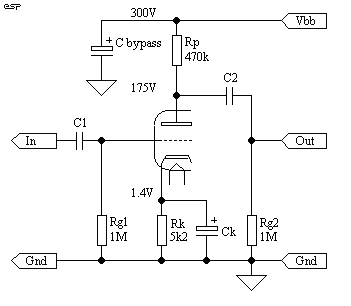
Figure 1.1 - A Basic
Valve Voltage Amplifier
This circuit configuration is known as "common cathode", because the cathode reference point (earth) is common to both input and output. By placing a resistor "Rk" in the cathode circuit, a voltage is developed because of the current flow. If the grid is referenced to earth (ground), then the grid is negative with respect to the cathode. The voltages shown on the circuit are typical of a single element of a 12AX7 twin triode. Note that the two valve pins that are not connected are for the heater. This is used to heat the cathode so that it emits electrons more readily.
The cathode resistor will cause the circuit to reach a stable current, where any attempt at increasing the cathode current will cause a greater voltage across the resistor, making the grid effectively more negative and reducing the current. A point of equilibrium is quickly reached, where the circuit operates in a stable manner. This is known as cathode biasing, and is most common with signal level and very low power amps.
By applying a varying voltage (the signal) to the grid, the current between cathode and anode will vary too. Since the anode load is a resistance, a varying voltage will be developed which will (hopefully) be greater than the voltage applied to the grid. The input voltage has been amplified.
Because the signal voltage on the grid is "fighting" the attempt of the cathode resistor to maintain the current through the valve at a constant value, this is a form of feedback. It is also known as cathode degeneration. The name is of no consequence, because as local feedback, it will improve the linearity of the stage but reduce the gain. In reality, the improvement in linearity is only minor, and leaving out the capacitor can increase noise in sensitive circuits - especially hum that is induced into the cathode from the heater, which was nearly always operated from AC in the past, but DC heater supplies are now common.
Where the cathode is directly heated (the filament has the oxide coatings directly applied), DC operation is mandatory, or hum would be inevitable. Directly heated cathodes will always emit electrons unevenly, because of the voltage gradient across the filament. The most postive end will have the greatest emission, since the negative voltage between cathode and grid is lowest.
Note that for indirectly heated cathodes, the heating element is called the heater, but for directly heated cathodes it is more commonly referred to as the filament (as in the heated filament of a light bulb).
Because valves have a relatively low voltage gain, it is common to bypass the cathode resistor with a capacitor to defeat the local feedback and extract as much gain as possible, as is shown in Figure 1.1. The gain (or more correctly, the transfer characteristic) of a valve is sometimes measured in mA/V - which tells us how many milliamps change in anode current will occur with a grid voltage change of 1 Volt. Another common way to describe this is "mu" or amplification factor. Yet another value is common with valves - the "conductance" (A.K.A. mutual conductance or transconductance), which is the opposite of resistance, and is expressed in Mhos (Ohms backwards - seriously!).
One problem with valves has always been the number of different methods used to describe what is essentially the same thing. Depending entirely which book you happen to be reading, you will see the effective gain quoted as mA/V, mutual conductance ("gm", in Mhos or more commonly uMhos), or the equally obscure term "Amplification Factor", none of which has any direct relevance to the gain you can expect without further calculation.
The output impedance of the circuit of
Figure 1.1 is 470k - the same as the plate resistor. Rg2 is the grid
resistor for the following stage, and at 1M, loads the output and reduces
gain.
There are three main characteristics that are quoted for any given valve. These are:
A typical signal valve (such as the 12AX7 high mu dual triode) has a plate resistance of 2k5, an amplification factor (mu) of 100, and a gm (using the circuit of Figure 1.1) of about 1600uMhos, which can (by simple mathematics) be converted into a figure of 1.6mA/V, meaning that a change of 1V on the grid will cause a change of 1.6mA in the anode current. This does not actually mean what it says, since the valve might be quite incapable of sustaining an anode current of 1.6mA under all circumstances. However, a change of 0.1V at the grid can cause a change in plate current of 0.16mA - the measurement is typically "normalised" to make comparison easier (just like they don't in the supermarket).
Let us now have a look at how the valve amplifies the signal. The transfer curve in Figure 1.2 shows the input waveform applied to the grid, at any convenient frequency. As the signal becomes more positive, the valve draws more current, until at the peak of the waveform, the grid voltage has been made 0.1V more positive than it was before. Therefore, the anode current is 0.16mA greater that it was before. Using Ohm's Law, 0.16mA with a resistance of 470k means that the anode voltage is 75 Volts lower than when in the idle (or quiescent) state.
This would seem to indicate that the valve has a gain of (75 / 0.1) 750 - not a chance! The circuit of Figure 1 will have a typical voltage gain (Av) of around 75. As I said - everything changes. The only way to be certain what a valve will actually do is consult the manufacturer's data, and refer to the transfer curves for the mode of operation you wish to use. Supply voltage, plate current, plate voltage and the impedance of the next stage all have a profound effect on the performance of a valve.
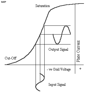
Figure 1.2 - Typical
Valve Transfer Curve
As can be seen from Figure 1.2, the transfer curve is not linear, which means that as the valve approaches cut-off (turned off completely) or saturation (turned on completely) the characteristics change, and distortion is introduced. A (very) rough estimation of maximum rms output voltage to keep distortion below 1% is about 0.1 of the quiescent plate voltage. Thus, with a plate voltage of 150V at idle, the maximum output voltage will be 15V RMS. This assumes that the valve has been biased correctly in the first place. From the graph we can see that at high values of negative grid voltage the valve will cut off, while at low (or positive) grid voltage, the valve is turned on as hard as it can.
A valve can be thought of as having an
infinite input impedance (although this is never realised in practice).
The input impedance is approximately equal to the value of the grid resistor
for audio frequencies. The output current is therefore controlled
by a voltage at the grid, so the valve migh be considered a voltage controlled
current source (or VCCS).
Figure 1.3 shows a valve current amplifier, commonly known as a cathode follower, or common plate (because the plate circuit is common to both input and output - for AC signals only). Although this circuit can provide a useful increase of current, and an equally useful decrease in output impedance, it has a voltage gain that is less than unity. Typically, this will be about 0.8 to 0.9, so for every volt of signal applied to the input, we only get about 850mV output.
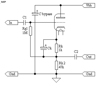
Figure 1.3 - Cathode
Follower Current Amplifier
The cathode follower is typically used where a low impedance output is desired, since the output impedance of most valve circuits is rather high (equal to the value of the plate load resistor). Simply attaching a low impedance load to a voltage amplifier stage will cause the output level to be dramatically reduced, so the current amplifier (cathode follower) is a useful stage. The output impedance of the circuit of Figure 1.3 can be expected to be about 1/10th the value of the cathode resistance Rk2 - but this is highly dependent on the valve itself, and its operating current. The available current is very low, so the circuit will not be able to drive a load much less than Rk2, or 47k. Remember that output impedance and drive capability are not related.
Note that the grid must still be biased
to an appropriate voltage negative with respect to the cathode. The
bypassed cathode resistor is used as before, but the grid is connected
to the bottom of this resistor, and not ground. If it were connected
to ground, the circuit would be capable of only very small signal levels
before it distorted.
Finally, we can combine a voltage amplifier stage and a current amplifier stage, and get a power amplifier. Cathode followers are very unusual in the valve amplifier, and it is more common to use a "push-pull" output stage, generally using a transformer to match the high voltage and relatively high impedance of the output valves to the impedance of the speaker.
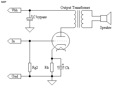
Figure 1.4 - Basic Valve
Power Amplifier
Figure 1.4 shows a very basic valve power amplifier, using a triode in "single-ended" mode. The output transformer converts the high voltage, high impedance plate circuit of the valve to a low voltage, low impedance signal for the loudspeaker. Because the primary of the output transformer must carry the full DC quiescent current of the valve (which will be a large, high current unit), it needs a very large core of laminated steel.
Interestingly, these inefficient and high distortion amplifiers have made a comeback in recent years. However in the heyday of the valve, the efficiency and distortion of these circuits was such that they were replaced in nearly all installations by more efficient and lower distortion circuits, such as that shown in Figure 1.5.
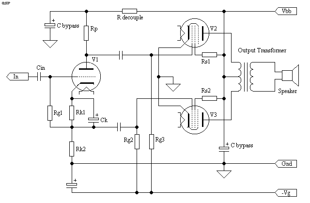
Figure 1.5 - Push-Pull
Valve Power Amplifier
The valves shown for the output are called pentodes (from penta - five), having 5 electrodes instead of the three for a triode. The second grid (called the screen grid, or just screen) increases the gain of the valve dramatically, while the third grid, the suppressor, prevents what is called "secondary emission" from the plate. The screen accelerates the electron flow so much that electrons bounce off the plate, or dislodge others. The addition of the screen gives the valve some nice characteristics, such as much higher gain, but also some nasty ones (lower linearity, more distortion), which the suppressor counteracts to some degree. The suppressor grid is almost always connected internally to the cathode. It is not uncommon for designers to connect pentodes as triodes, by connecting the screen and plate together.
The first stage of the circuit is interesting, and is called a phase splitter. It is a combination of a voltage amplifier and a current amplifier, having equal values of resistance in each circuit (i.e. Rp = Rk2). Because all valves have the same "polarity", they cannot be used like transistors or MOSFETs, but must be driven with their own signal of the correct polarity.
The incoming signal is therefore sent "as is" to one valve (from the cathode circuit), and is inverted for the other - hence the term push-pull. As one valve "pushes" the anode current lower, the other simultaneously "pulls" it higher. In a properly designed circuit, the two output valves will pass the signal between them with little disturbance. Any disturbance in this region is called crossover distortion, because it happens as the signal crosses over from one valve to the other.
Notice something else quite different. The cathodes of the output valves are connected directly to earth, and the grids are supplied with a negative bias from a separate -ve power supply. This is the most common method of biasing output valves in high power circuits, having a much greater efficiency than cathode biasing.
For many large output valves, it is not
even considered a good idea to use cathode biasing, because the amount
of negative grid voltage required is too high. Voltages of up to
-60V are not uncommon with high power pentodes or another common type,
beam power tetrodes (I will not cover these in more detail, but there is
much information to be found on the web). Using cathode bias for
this sort of voltage is inefficient and reduces the output power dramatically.
The above is but a very small offering from the world of the vacuum tube. As I said in the introduction, this is not designed to be a complete electronics training course. The circuits presented are basic only, which is to say that they will all work, but are not optimised in any way.
For further reading, the most highly recommended work is the rather old (but still considered the reference manual) "Radiotron Designer's Handbook", by F. Langford-Smith and originally published by Amalgamated Wireless Valve Co. Pty. Ltd. in Australia. My copy is dated 1957, but it has recently been republished (although I think it is quite expensive, unfortunately).
Overall, the valve is still an almost mystical thing, but in all honesty, modern amplifiers using transistors or MOSFETs are so vastly superior in terms of fidelity, efficiency and reliability, that I really don't see what all the fuss is about. Having said this, I am using a valve preamplifier on my own system.
There is no doubt that valves do have some very nice characteristics, and for guitar amplifiers there are few guitarists who would argue otherwise. A soft overload behaviour means that a valve amp does not sound as harsh as a transistor amp when it is overdriven - which is great for guitar, but a hi-fi should never be overdriven anyway, so the point is moot.
The problems that befall valves are many, and include
At low levels, valve equipment has vanishingly
small distortion levels, and when all is said and done, there is something
nice about little glass tubes, with little lights inside, making your music.
Since it was invented, the transistor (from "transfer resistor") has come a long way. Early transistors were made from germanuim, which was "doped" with other materials to give the desired properties required for a semiconductor. In the beginnings of the transistor era, nearly all devices were PNP (Positive Negative Positive), and it was very difficult to make the opposite (NPN) polarity. The NPN transistors that were available at that time were low power and did not work as well as their PNP counterparts.
When silicon was first used, the opposite was the case, and for quite some time the only really high power devices available were all of silicon NPN construction. More recently, it has become possible to make NPN and PNP transistors that are almost identical in performance. Germanium is rarely used, although some examples are still available.
All transistors have three "elements":
Since the base to collector junction is reverse biased in normal operation, there will be no current flow. It is the action of injecting current into the base that causes current flow in the collector circuit. I do not intend to explain the exact conduction mechanism, as it is somewhat outside the scope of this article.
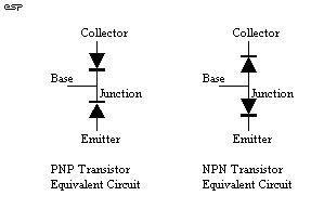
Figure 2.1 - Analogous
Depiction of Transistors
This is very convenient, because it gives us an easy way to check if a transistor is likely to be good or bad, simply by measuring the "diodes". Early PNP germanium devices would actually work equally well if the emitter and collector were reversed, but devices are now optimised to maximum performance, so this trick is not as successful (it does still work, but the device gain is MUCH lower when the terminals are reversed).
To make the transistor actually do something useful, it is necessary to bias it correctly. This is done (having selected a suitable collector resistance) simply by applying enough base current to ensure that the collector is at 1/2 the supply voltage. In the same way that the plate load resistor determines the output impedance of a valve amplifier, the collector resistor determines the output impedance of a transistor amplifier. Unlike a valve, the transistor is not said to have a "collector resistance" as in the equivalent resistance between emitter and collector, because this is not relevant to the operation of a transistor.
Figure 2.2 shows three methods of biasing a transistor. Of these Figure 2.2a is the least usable, because there is no mechanism to ensure that the circuit will be repeatable with different devices or with temperature. Variations caused by temperature are (and always have been) a real problem, and it is necessary always to ensure that the circuit has some feedback mechanism for DC operating conditions to ensure stability. Different transistors (of the same type and even from the same manufacturing run) will have different gains, and this, too, must be compensated for.
Assume that the gain of the transistor is 100 (exactly). This means that for 1mA of base current, 100mA of collector current will flow. The emitter current is the sum of the base and collector currents. To bias the transistor we need only meet this criterion (in theory), and everything will be well. With a Supply voltage (Vcc) of 20V, we want to have 10V at the collector, to allow maximum voltage swing. This will allow the voltage to go to +20V or to 0V, however the signal will be badly distorted by then.
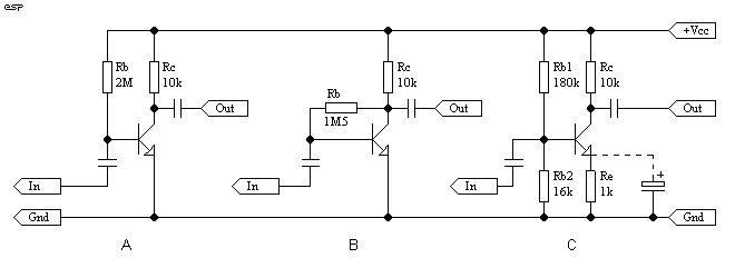
Figure 2.2 - Biasing
a Transistor Voltage Amplifier, Three Methods
Figure 2.2b is a simple way to achieve this, but has some drawbacks. Because the bias resistor (Rb) is supplied from the collector circuit, it will have some of the collector current flowing in it. This will introduce negative current feedback, which at DC stabilises the circuit, but with the AC signal makes the input impedance very low, as well as reducing gain for any finite value of source impedance. This is not necessarily a drawback, however, as the feedback also reduces the distortion components.
This problem is overcome with the circuit in Figure 2.2c, with a bias divider providing a fixed voltage reference, and the emitter resistor (Re) providing stabilising feedback as we saw with the valve voltage amplifier. In the same way as with a valve, this also provides feedback, increasing linearity and reducing gain. With a transistor we get one additional effect - the input impedance is increased (more on this subject later). Again, to achieve maximum gain, it is common to place a capacitor in parallel with Re to defeat the feedback for AC signals, allowing maximum gain.
To bias a PNP device, we use exactly the same circuitry, but the supply polarity is reversed, so the collector (and base) will have a negative voltage with respect to the emitter.
One of the major differences between valves
and transistors is that once we have decided on a suitable biasing circuit
(or specified a gain from the amplifier), we can make device substitutions
with little or no change in performance, provided the transistors have
similar basic parameters. Often the same circuit will work just as
well with perhaps 10 or 20 different devices, all from different manufacturers.
I shall only discuss the basic characteristics of transistors (as with valves), and there is really only one variable parameter and two fixed parameters (which are the same for every silicon transistor) to deal with. With transistors, the parameters are not as interactive as with valves, and the circuit gain is not as reliant on the device gain as with valves. In the same way as with valves, there are small signal devices (low power), working all the way up to power devices, which can have collector current ratings of 50 to over 100A for some of the very large power transistors.
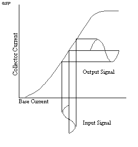
Figure 2.3 - Transistor
Transfer Characteristics
The signal transfer curve is similar to that of a valve, and is shown in Figure 2.3. There is generally less distortion in the linear part of the curve, but because of the lower operating voltage, a transistor amp must work closer to the supply rail and earth, so distortion is often much higher with simple circuits such as those in Figure 2.2 than with an equivalent valve amplifier.
The major cause of distortion in small signal transistor amplifiers is the variation in the internal emitter resistance (re). Because transistors can tolerate a wider range of supply voltage and operating current than valves, it was common (when transistors were new and frightfully expensive) to try to extract as much voltage gain as possible from each device. This is no longer an issue, but the problem is still there, and it is necessary to take steps to prevent distortion. Very high gain circuits with global feedback are extremely common with transistor circuits, which renders the circuit immune from almost any variation of the device parameters, whether intrinsic (internal fixed) or manufacture dependent.
The gain of a transistor stage is approximately equal to the collector resistance divided by the emitter resistance (including the internal resistance re). So for the circuit of Figure 2.2c, the gain will be 9.75 without the emitter bypass capacitor, or about 384 with it installed. The distortion will be much higher with the emitter bypass in place, and it is uncommon to see these circuits any more.
The input impedance of a transistor voltage amplifier is low, and the output impedance is determined by the collector resistance (ignoring any feedback that may be applied from collector to base).
The input impedance is essentially determined by the gain of the device, and the value of emitter resistance (including the internal resistance), and in theory (that word again) is approximately equal to the emitter resistance multiplied by gain. The circuit of Fig 2.2a will therefore have an input impedance in the order of 2600 Ohms, Fig 2.2b will be very low because of the feedback, and 2.2c (without the bypass capacitor) will have an input impedance of 100k - but as this is shunted by the bias resistors, the impedance will actually only be about 12k.
A transistor can be thought of as
a current controlled current source (CCCS).
The current amplifier is much more common in transistor circuits than with valves, and is called an emitter follower (or occasionally common-collector). The emitter follower (like the cathode follower) has a voltage gain of less than 1 (or unity), but the difference is much less. Typically, the gain of an emitter follower circuit will be about 0.95 to 0.99 - depending on the operating current. The use of feedback to lower this further is very common, and output impedances of less than 1 Ohm are quite possible.
Figure 2.4 shows a standard configuration for an emitter follower current amplifier stage. It is common to bias the base to exactly 1/2 the supply voltage, using equal value resistors. I say "a" standard because there are many different configurations that can be (and are) used, including direct coupling, which is very common with transistor circuits.
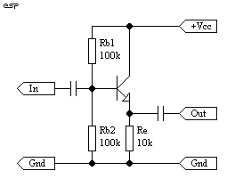
Figure 2.4 - Transistor
Current Amplifier
One of the great attractions of transistors is their flexibility, which is considerably enhanced by having two polarities of device to work with. Because of this, circuits such as that shown in Figure 2.5 are common (or they were before the advent of opamps). Indeed, opamps themselves use the flexibility of transistors to the full, as can be seen if you have a look at the "simplified equivalent circuit" often published as part of the specification sheet for many opamps.
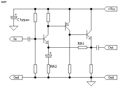
Figure 2.5 - A Typical
Direct Coupled Transistor Amplifier
As can be seen, this amplifier uses an emitter follower for the output, is direct coupled within the circuit itself, uses both NPN and PNP devices, and has feedback to set a gain which is dependent only on the ratio of the two resistors Rfb1 and Rfb2. It is this sort of circuit that the opamp came from in the beginning, and there are still ICs (and small power amplifiers) that use similar circuitry internally. Regular readers may even recognise the basic circuit from the Projects Pages - essentially this is a discrete opamp, and will have a very high gain, which is brought back to something sensible by the feedback.
The actual gain is almost entirely dependent
on the resistor values (for gains less than about 50 or so), and may be
calculated by
Av = (Rfb1 + Rfb2) / Rfb2
where Av is voltage gain (Amplification, voltage)
So to obtain a gain of 20, Rfb1 would be
22k, and Rfb2 1k2 - this is actually a gain of 19.33, representing an error
of 0.3dB. This gain is so stable that a completely different set
of transistors from a different manufacturer would make no difference to
measured gain performance. Other factors, such as noise or distortion
must vary with the quality of the active devices, but the changes will
generally be very subtle, and may not be noticeable at all, depending on
the similarity of the transistors.
A transistor power amplifier uses (typically) another configuration for the input stage. This is called a "long tailed pair", (LTP) and acts as both the input stage and error amplifier (Q1 and Q2). This circuit operates in current mode, so there is little output voltage to be seen from its output.
The second stage (Q3) is a Class-A amplifier, and is responsible for a large proportion of the overall gain of the circuit. Notice the current sources that are typically used for the LTP and Class-A amp sections. These are commonly made using transistors and maintain a constant current regardless of the voltage at the collector. If the current were truly constant, this implies that the impedance is infinite (which means that the gain of the transistor stage is also infinite!), and although this is not the case in reality, it will still be remarkably high.
For more information on how current sources are constructed, see Section 5.1
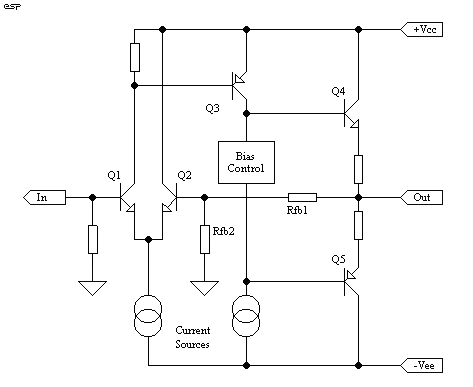
Figure 2.6 - Transistor
Power Amplifier
The output stage (Q4 and Q5) typically is a pair of complementary emitter followers, which must be correctly biased to ensure that as the signal passes from one transistor to another, there is no discontinuity. This form of operation is known as Class-AB, since the amp operates in Class-A for very low level signals, then changes to Class-B at higher levels. Any discontinuity while passing the signal from one transistor to the other is the cause of crossover distortion, and for many years gave transistor amplifiers a bad name in the audio world. With proper biasing, and properly applied feedback, the crossover distortion can be made to go away - although never completely, but amplifiers with distortion levels of well below 0.01% are common.
The resistors at the emitters of the output transistors help to maintain a stable bias, and also introduce some local feedback to linearise the output stage. This is a simplified circuit, and in reality the output stage will usually consist of multiple transistors, commonly a driver transistor followed by the output transistor itself. This does not change the operation of the circuit, but simply gives the output stage more gain, so it does not load the Class-A driver too heavily (this will result in greatly increased distortion).
Like the previous example, the gain is entirely dependent on the ratio of Rfb1 and Rfb2. As shown, the amp in Figure 2.6 is DC coupled, meaning that it will amplify any voltage from DC up to its maximum bandwidth. Not shown on this circuit are the various components needed to stabilise the circuit to prevent oscillation at high frequencies - often in the MHz range. Such oscillation is a disaster for the sound, and will quickly overheat and destroy the output transistors.
There are also transistor amplifiers that
operate in Class-A, which means that the output transistors conduct all
the time, and are never turned off. This can produce distortion levels
that are almost impossible to measure, but this is at the expense of efficiency,
and Class-A amplifiers will get very hot while doing nothing. Unlike
the more common Class-AB amplifier, they will actually get slightly cooler
as they reproduce a signal, since some of the input power is then diverted
to the loudspeaker.
Just as with valve amplifiers, I have only scratched the surface. Entire books are written on the subject, and range from basic texts used in technical schools, to very advanced tomes intended for university students. Since transistors are easy to work with (and safe), there is much to be gained by experimentation, and you will have the satisfaction of having designed and built a functioning amplifier.
Transistors also have their fair share of problems, and there are some things that they are just not very good at. Some of the major failings include:
They are also very quiet (generally much quieter than valve amps) and do not suffer from microphony, so room vibrations are not re-introduced into the music. Efficiency is much higher, with lower voltages and no heaters (its a pity they don't look really nice, though).
Output impedances of 0.01 Ohm are achievable, so loudspeaker damping can be very high. Because transistor amps are very mechanically rugged, they can be installed in speaker boxes, so speaker lead lengths can be very short.
Typical transistor amplifiers have much
wider bandwidth than valve amps, because there is no transformer, this
is especially noticeable at the lowest frequencies - a transistor amp can
reproduce 5Hz as easily as 500Hz
Now on to FETs and MOSFETs. FET stands for Field Effect Transistor, and MOSFET means Metal Oxide Semiconductor Field Effect Transistor. This topic is something of a can of worms, not because of some deficiency in the devices, but because of the huge array of different types. The basic FET types are
FETs are "unipolar" devices, in that they use only one polarity of carrier, in contrast to bipolar transistors, which use both majority and minority charge carriers (electrons or "holes", depending on the polarity). FETs are far more resistant to the effects of temperature, X-Rays and cosmic radiation - any of these can cause the production of minority carriers in bipolar transistors).
I shall concentrate only on three terminal FETS, and the terminals are
The junction FET is common in the inputs of high performance opamps, and offers extremely high input impedance. Indeed this is the case for discrete FETs as well, and a simple voltage amplifier using a junction FET and a power MOSFET are both shown in Figure 3.1. Both devices are N-Channel, and note that the arrow points in a different direction for each. The arrows point in the opposite direction for a P-Channel device, and all polarities are reversed. Vdd is +20V.
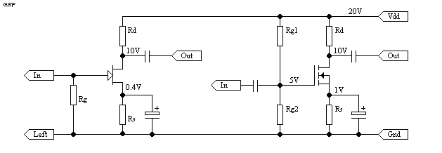
Figure 3.1 - Junction
FET and Power MOSFET Voltage Amplifiers
Junction FETs are depletion mode devices, and (like all depletion mode FETs and MOSFETs) can be biased in exactly the same way as a valve. Depletion mode means that without a negative bias signal on the controlling element (the gate), there will be current flow between the drain (equivalent to plate or collector) and source (equivalent to cathode or emitter).
An enhancement mode device remains turned off until a threshold voltage is reached, after which the device conducts, passing more current as the voltage increases. Although there are MOSFETs made for low power operation, the majority (in audio, anyway) are power devices. These are almost exclusively enhancement mode, and can be capable of very high current.
In Figure 3.1, the power MOSFET is an enhancement mode device, and the junction FET is depletion mode. These are the most commonly used in audio. Enhancement mode power MOSFETs are also used in switching power supplies, and are far better than bipolar transistors in this role. They are faster, so switching losses are not as great (therefore the MOSFETs run cooler), and they are more rugged, and able to withstand abuses that would kill a bipolar transistor almost instantly.
This ruggedness (coupled with the complete freedom from second breakdown effects), means that MOSFETs are very popular as output devices for high power professional amplifiers. In this area, the MOSFET is second to none, and they are firmly entrenched as the device of choice for high power.
This is not to say that this is the only place MOSFETs are used. There are many fine audiophile power amps (and even preamps) that use power MOSFETs, and there are many claims that they are sonically superior to bipolar transistors (again, a debate that I will not discuss here).
Somewhat like valves, FETs and MOSFETs
are very device dependent, and it is not normally possible to just substitute
one device for a different type. Also like valves, the gain that
can be expected from a voltage amplifier circuit is device dependent, and
the manuafcturer's data sheet (or testing) is the only way that one can
be sure of obtaining the gain required in a given circuit.
The characteristics of FETs must be covered in two parts, since we are dealing with two quite different devices. The first will be the junction FET, and as with transistors, I shall only describe the N-Channel, but virtually identical P-Channel devices are available (although not as commonly used).
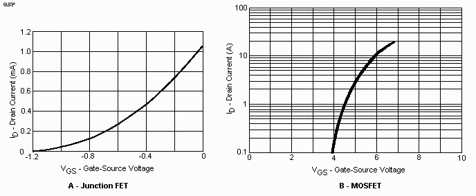
Figure 3.2 - Transfer
Curves For a Junction FET and MOSFET
Initially, so the transfer characteristics of the two devices can be seen side by side for comparison, Figure 3.2 shows a fairly typical device from each "family" The junction FET data is from a 2N5457, and the MOSFET is an IRFP240.
Rather than show the input and output signals superimposed on a graph, this time I show only the graph itself. These are excerpts from manufacturers data, but with a small catch - Figure 3.2b has the drain current displayed on a logarithmic scale, so the linearity of the device cannot be seen properly. If this graph were redrawn as linear, it will show that linearity is best at higher currents (on the graph shown it looks the other way around), and the device becomes almost perfectly linear with drain currents above about 3A
Note that because the junction FET is depletion
mode, drain current is highest at 0V gate-source voltage. The MOSFET
on the other hand is enhancement mode, so at 0V gate-source, there is no
current. Conduction starts at 4V, and by 6V the drain current is
10A.
| The term Siemens (S) is now replacing Mhos as the unit of transconductance in some literature: 1S = Mho (1uS=1 uMho. For the above graphs, it may be worked out that the junction FET has a transconductance of 1500uS, and for the MOSFET it is approx. 9,000uS (9,000 uMhos) |
Junction
FETs
Like valves, FET data sheets provide gain
information as gm (mutual conductance - in uMhos). The junction FET
shown has a gm of (typically) 1,500 uMhos (in the graph shown it is actually
closer to 1425 uMhos in the linear section), which translates to about
1.5 mA/V.
The most common of the quoted parameters for junction FETs are
FETs offer low noise, especially with high impedance inputs, and in this respect are the opposite of bipolar transistors, which are generally at their best with low source impedance.
Junction FETs are predominantly low power, although there are some high power devices available. These are uncommon in audio applications.
MOSFETs
Again, MOSFET data sheets also provide
information similar to junction FETs, but there are more items of importance
to the designer. The most useful of these are
At increasing gate voltages, the drain current increases until either a) the maximum permissable drain current or total dissipation limit is reached, or b) the drain voltage falls to its lowest possible value. In this instance, since the source-drain channel is now fully conducting, the value of RDS(on) determines the voltage.
Typical power MOSFETs offer extremely low on resistance, with values of 0.2 Ohm being fairly typical. There are some devices with much lower values, but this is only important in switching circuits. In an audio amp, the MOSFETs should never be turned completely on, since this means the amplifier is clipping.
Another area that must be addressed with
MOSFETs is the voltage between gate and source. Because the gate
is insulated from the channel by a thin layer of metal oxide, it is suceptible
to damage by static discharge or other excessive voltage. It is common
to include a zener diode between source and gate to ensure that the maximum
voltage cannot be exceeded. Voltage spikes in excess of the breakdown
voltage of the insulating layer will cause instantaneous failure of the
device.
Again, I have shown both a junction FET and a MOSFET in Figure 3.3, both common-drain or source-follower circuits. As can be seen, the junction FET is biased almost identically to a valve, but all voltages are much lower. The MOSFET requires a positive voltage, and this must be greater than the source voltage, by an amount that takes the characteristics of the MOSFET into consideration. For the device characteristics shown in Figure 3.2 this means that at a current of 100mA, the gate must be 4V higher than the source.
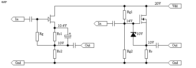
Figure 3.3 - FET Current
Amplifiers
Included in the MOSFET version is a zener
for protection of the gate insulation. A 10V zener is used, as this
gives good protection and is still able to let the maximum possible MOSFET
current flow. A 6V zener could have been used, and this would still
allow current up to 10A, which is far more than can be achieved from this
simple circuit.
In exactly the same way as a power valve can be used in single-ended Class-A, so too can a MOSFET. A simple circuit is shown in Figure 3.4 which will provide about 10W of audio. Using a constant current source as a load (as shown) gives much better efficiency than a resistor, and improves linearity. The distortion from a circuit such as that shown will be roughly the same as that from a single ended triode valve circuit. Overall efficiency will be higher, since there is no cathode bias resistor needed, and no heaters as with a valve.
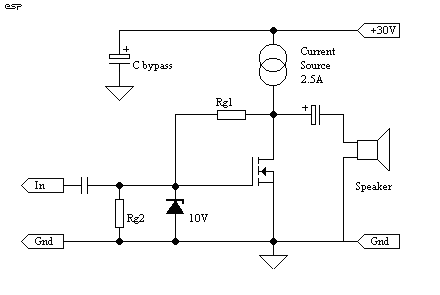
Figure 3.4 - Single Ended
MOSFET Class-A Amplifier
Although there are a few, all MOSFET power amplifiers are uncommon. Most use a combination of bipolar transistors (for the input and gain stages), and MOSFETs for the output devices. This seems to be the most popular circuit arrangement, so I will concentrate on this. Figure 3.5 shows a fairly typical arrangement (in simplified form), and the operation of this is almost identical to that of an amplifier using bipolar transistors in the output. Note that emitter followers are needed to be able to provide the low impedance drive that MOSFETs need, although in some circuits they are not used. Instead, the Class-A driver stage (Q3) is operated at a higher than normal current to allow it to drive the MOSFETs properly.
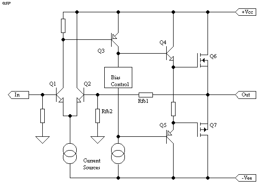
Figure 3.5 - MOSFET Output
Power Amplifier
One problem with this arrangement is that the drain to source voltage represents a circuit loss, so the power supply voltage needs to be typically +/-6V higher than the required peak output voltage to the load. Although this is not a major problem, it does increase dissipation in the output stage, and the loss increases with lower impedance loads.
Some (especially very high power) amps get around this by using a low current (but higher voltage) secondary power supply for the drive circuit, and the main high current supply for the MOSFETs. In an amp using +/-50V at 20 Amp main supplies, the secondary supply might be +/-60V, but capable of perhaps 1A maximum.
As with the bipolar amp (did you notice
how similar they are?), I have not included components for stability.
These are typically the same as for a standard bipolar transistor amp,
but will usually include "stopper" resistors in series with the gates of
the MOSFETs, and sometimes additional capacitance to prevent parasitic
oscillation - the need for these varies from one device type to the next.
Junction
FETs
The surface is again, only barely scratched.
The junction FET (A.K.A. JFET) is ideally suited to circuits where high
impedances are expected, and will give the lowest noise. They are
an invaluable electronic building block when used where they excel - providing
extremely high input impedance.
Like all devices so far, JFETs have their limitations
JFETs (in fact all FETs) are more sensible than bipolar transistiors when heated, and problems of thermal runaway are not encountered with these devices.
MOSFETs
The MOSFET is one of the most powerful
of all the current range of amplifying device, with extraordinary current
capability. Ideally suited to very high power amplifiers, where extremes
of operating conditions are regularly encountered, the MOSFET has no equal.
... And, as always, there are limitations
Coupled with a positive temperature coefficient that completely stops thermal runaway in a linear circuit, the MOSFET is almost indestructible, provided that precautions are taken to ensure the gate voltage is kept below the breakdown voltage.
The positive themerature coefficient is
a great help in audio circuits, although it can be a problem in switching
power supplies, since the "on" resistance also increases with temperature,
and in a switch-mode power supply this can cause thermal runaway (exactly
the reverse of bipolar transistors in this application).
No discussion of amplifying devices would be complete without a discussion of opamps. Although not a single device, the opamp is considered to be a building block, just like a valve or any transistor.
The format I used for the other discussions is not appropriate for this topic, so will be changed to suit this most versatile of components. I shall not be covering esoteric or special purpose types, only the basic variety, as there are too many variations to cover.
The operational amplifer was originally used for analogue computers, although at that time they were made using discrete components. Modern (good) opamps are so good, that it is difficult or impossible to achieve results even close with discrete transistors or FETs. However, there are still some instances where opamps are just not suitable, such as when high supply voltages are needed for large voltage swings.
The majority of power amplifiers (whether bipolar or MOSFET) are in fact discrete opamps, with a +ve input and a -ve input. You tend not to see this, but have a look at Figure 3.5 again. The signal is applied to the +ve input at the base of Q1. The base of Q2 is the -ve input, and is used for the feedback signal, exactly the same as you will see in Figure 4.1a below.
Unlike the other devices, opamps are primarily designed as voltage amplifiers, and their versatility comes from their input circuitry. Opamps have two inputs, designated as the non-inverting and inverting (or simply + and -).
When wired into a conventional amplifier
circuit, the opamp has one major goal in its little life ...
Make both inputs
the same voltage
If, because some swine of a designer has
made this impossible (very common with a lot of circuits), the opamp then
takes another approach ...
Make the output
the same polarity as the most positive input
The latter condition needs a small explanation. If the +ve input is most positive, then the output will swing to the positive supply rail (or as close as it can get). Should the -ve input be more positive, then the output will swing to the negative supply rail. The difference between the two inputs may be less than 1mV! Simple as that.
I call these "The First and Second Laws of Opamps". These two statements describe everything an opamp does, and just by knowing this, makes the task of working out what most common circuits do a simple process. There is actually nothing especially complex about opamps, unless you look at the "simplified" circuit diagram often included in data sheets. Don't do this, as it is too depressing. (By the way, the first statement is not strictly true of real-life devices, which will always have some error, however without very specialised equipment you will be unable to measure it.)
Modern opamps (the good ones, anyway) are as close as anyone has ever got to the ideal amplifier. The bandwith is very wide indeed, with very low distortion (0.00003% for one of the Burr Brown devices), and low noise. Although it is quite possible to obtain an output impedance of far less than 10 Ohms, the current output is usually limited to about +/-20mA or so. Supply voltage of most opamps is limited to a maximum of about +/-18V, although there are some that will take more, and others less.
Depending on the opamp used, gains of 100 with a frequency response up to 100kHz are easily achieved, with noise levels being only very marginally worse that a dedicated discrete design using all the noise reducing tricks known. The circuits shown below have frequency response down to DC, with the upper frequency limit determined by device type and gain.
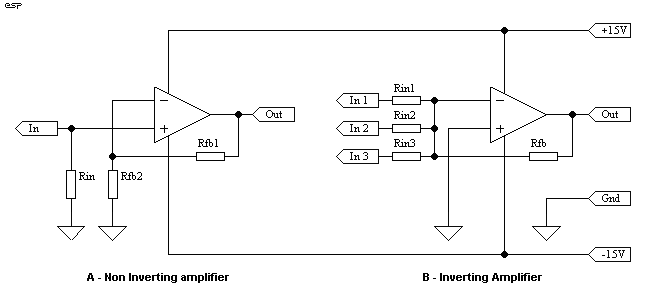
Figure 4.1 - Standard
Opamp Configurations
Figure 4.1 shows the two most common opamp amplifier circuits. The first (4.1a) is non-inverting, and is the better connection for minimum noise. The voltage fed back through Rfb1 will cause a voltage to be developed across Rfb2. The output will correct itself until these two voltages are equal at any instant in time. It does not matter if the signal is a sinewave, square wave, or music, the opamp will keep up (provided you stay within its capabilities). Once the speed of the opamp is not significantly higher than the rate of change of the input (generally a factor of 10 is sufficient - i.e. the opamp needs to be 10 times faster than the highest frequency signal it is expected to amplify), the output will become distorted. At voltage gains of 10 or less, almost any opamp will be able to keep up with typical audio signals, but (and be warned) this is no guarantee that they will sound any good.
Input impedance is equal to Rin, and voltage
gain (Av) is calculated from
Av = (Rfb1 + Rfb2) / Rfb2
The second circuit (4.1b) is an inverting amplifier, and is commonly used as a "summing" amplifier - the output is the negative sum of the three (or more) inputs. It is also called a "virtual earth" mixer, because the -ve input is a virtual earth (remember my "First law of opamps"). If the +ve input is earthed (grounded), then the opamp must try to keep the -ve input at the same voltage - namely 0V.
It does this by adjusting its output until the current flowing through Rfb is exactly the same (but of the opposite polarity) as the current flowing into the inputs from each Rin. They must all sum to 0V, as they are equal and opposite. This is done with amazing speed, and good opamps will continue to succeed in fulfilling the First Law up to over 100kHz or more (depending on gain). Lesser devices will start to have trouble, and the appearance of a measurable voltage at the -ve input is an indication that the opamp can no longer keep up with the signal.
Input impedance is equal to RinX (where
X is the number of the input), and voltage gain is calculated from
Av = Rfb / RinX
Multiple inputs can all have different gains (and input impedances). There are two catches to this circuit. The first is that if the source does not have an output impedance significantly lower than Rin, then the gain will be lower than expected. The other, not always realised, is that if the circuit is configured for a gain of 1 (actually it is technically correct to refer to it as -1), Rin1, Rin2 etc. will all be equal to Rfb. If the circuit has 10 inputs, then from the opamp's perspective it has a gain of 10, and its frequency response and noise will reflect this.
There are literally hundreds of different opamp circuit configurations. Feedback circuits with frequency dependent components (capacitors or inductors) make the opamp into a filter, or a phono equaliser, or almost anything else.
Power Opamps
Opamps even come in power versions, using
a TO-220 (or other specialised) case, and are typically capable of around
25W into an 8 Ohm speaker load. These devices, while not exactly
to audiophile standards, are still very capable, and have been used by
many domestic appliance manufacturers in such things as high-end TV sets
and standard hi-fi equipment. Some of the more advanced devices are
capable of output power up to 80W.
They typically have distortion figures
below 0.1%, and can be used anywhere a small, convenient and cheap power
amp is required. The circuit looks almost identical to that of a
small signal opamp, except that a zobel stabilisation network is used on
the output to prevent oscillation.
There are some circuits in the world of electronics that are just too useful. While some have been around for many years, others only became practical with the advent of the transistor. The circuits described are a mixture, some are very old, and others much newer.
I shall not go into the history (this is an electronics tutorial, not a history lesson), but will show the various stages in their basic form for each type of circuit.
On the topic of current sources, sinks
and mirrors, click here to see
the full article describing how they are most commonly used in audio circuits
(and why).
The constant current source (or sink) is one of the most versatile and widely used of the circuits shown in this section. The ideal current source provides a current into a load that is independent of the resistance (or impedance) of the load, from zero to infinity. As always, the ideal does not exist, but within the capabilities of the power supply voltage, it is quite simple to do, and surprisingly accurate.
There is no real difference between the two circuits - one sources current (or sinks electrons) or vice versa. Sometimes it might help to consider the circuit "upside down" to see that there is no real difference, only one of terminology.
As an example, if we wanted to supply a current that were fixed at 1A into any load impedance, then we might use a circuit similar to that in Figure 5.1 - a basic transistor current source. As shown, this will supply 1A into any resistance from zero Ohms up to a little under 50 Ohms. The power supply is the limiting factor - to be able to supply the same current into 1M Ohm would need a 1,000,000V power supply, which is an unrealistic expectation.
The current source or sink can be imagined as a device with infinite impedance - this must be the case if the current remains unchanged even as the load resistance is varied over a wide range. Naturally, the impedance of actual current sources is not infinite, but can easily reach values of many megohms, even in a simple circuit.
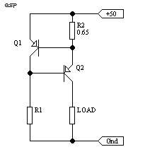
Figure 5.1 - A Basic
Transistor Current Source / Sink
The operation of the circuit is simple. If the voltage across the emitter resistor of Q2 attempts to exceed 0.65V (the base turn-on voltage for a silicon transistor), then Q1 will turn on, and short out all base current to Q2 except for exactly that amount required to maintain the specified current of 1A. If the collector current of Q2 falls, then the voltage across the emitter resistor also falls. This turns off Q1 until the current is again stable at the preset value. (This is only one way to make a current source - there are many others.)
Thermal stability is not good. The emitter-base potential falls at 2mV / degree C, so as the temperature increases, the current will fall from the nominal 1A. At low temperatures, the opposite will occur. A precision voltage reference can be used, or an opamp can monitor the voltage across the resistor, resulting in a much more stable current. Fortunately, in most circuits, it is not that critical, so the circuit of Figure 5.1 is very common.
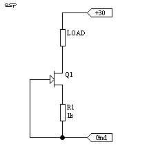
Figure 5.2 - A JFET Current
Source / Sink
Junction FETs, being a depletion mode device,
can be used as a current source very easily, as shown in Figure 5.2.
Because JFETs are mainly low current devices, the useful range is from
about 0.1mA up to 10mA or so. This is ideal for many of the circuits
that need a current source. The actual current is dependent on the
FET's characteristics, but is sufficiently stable for many non-critical
applications. Based on the FET curve shown in Figure 3.2a, this current
source will supply a current of about 0.4mA into a load from zero to 72k
Ohms. The voltage is also lower, because of the lower voltage rating
of most FETs.
The current mirror is one of the "new" circuits, and works well with bipolar transistors. It is unusual to see this circuit implemented with valves or FETs, and I will not change this (i.e. I will show transistors only). Figure 5.3 shows a simple current mirror (this version is not very accurate, but is still extremely effective and commonly used).
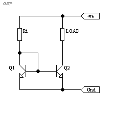
Figure 5.3 - A Simple
Current Mirror
Any current injected into the collector/base
circuit of Q1 (via Ri) will be "mirrored" by Q2, which will draw the same
current through its load resistor (within the capability of the transistor
and power supply). Current mirrors are sometimes used as current
sources (one less resistor), and are not as dependent on temperature, since
both transistors will ideally be at the same temperature. It is not
uncommon to use dual transistors (or thermal bonding) to ensure stability.
The long tailed (or differential) pair is an old circuit, and is used with valves, FETs and BJTs. It was originally designed in the valve era, and provides a means for the comparison of two voltages. The long tailed pair (LTP) is used as the input stage of most opamps, and many (if not most) modern power amplifiers.
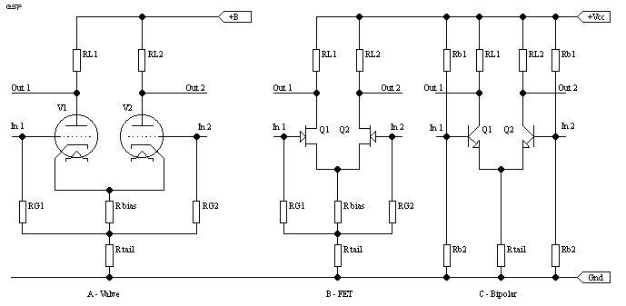
Figure 5.4 - The Long
Tailed Pair - All Common Devices
As can be seen in Figure 5.4, the LTP can be made using valves (A), JFETs (B) or bipolar transistors (C). Valves and JFETs can be self biased as shown, but BJT circuits must have external bias resistors. A pair of MOSFETs could be used, but at the typical currents used (less than 5mA), the gain and linearity would be very poor. Although each circuit is shown using a resistor as the "tail", in FET and bipolar circuits this is most commonly a current source (or sink if you prefer).
The use of a current source stabilises the overall current, so the device input current is not affected by supply voltage changes, or variations in the input bias voltages.
In each case, the circuit has an inverting and a non-inverting input, and an inverted and non-inverted output. Application of the same voltage and polarity to both inputs at once results in (theoretically) zero output - this is called the common mode signal, and is commonly quoted for opamps as the common mode rejection ratio.
The valve and FET versions only require capacitive coupling, as they are self biasing as shown. The bipolar circuit cannot be self biased, and requires the biasing resistors Rb1 and Rb2 for each input.
The output of each version may be taken from either or both outputs, and may be capacitively or direct coupled. Direct coupling is very common with LTP circuits, especially in opamps and audio power amplifiers, where it is the rule, rather than the exception.
When used as the input stage of an amplifier,
the LTP uses one input as the signal input, and the other is used for the
application of feedback, in the same way as in an opamp.
Sometimes, it is desirable to have an extremely low input impedance, for example where the output impedance of the source is very low. One way to achieve this is to use the control element (grid, gate or base) as the reference, and apply the signal to the cathode, source or emitter (as appropriate). Figure 5.5 shows an example of grounded (or common) grid (A), gate (B) and emitter (C).
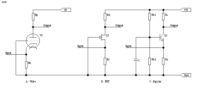
Figure 5.5 - Common Grid,
Gate and Base Amplifiers
Apart from having an extremely low input impedance, this class of amplifier has an additional advantage. The normal capacitance from output to input is bypassed to earth, and no longer acts as a feedback path. Such circuits are therefore capable of a much better high frequency response than when used in the "conventional" way, and are common in radio frequency circuits. The bypass path is direct for a valve or FET, and is via a capacitance for the bipolar circuit.
All inputs and outputs must be capacitively coupled, unless the preceding circuit is to be direct coupled (unusual) or the output is direct coupled to a follower (quite common).
Because the input impedance is so low,
there are few applications in audio, except where this circuit is used
in conjunction with a "normal" amplifier stage. This forms a new
circuit, called cascode.
This circuit was developed in the valve era, primarily to obtain better response at high radio frequencies. Valves have capacitance between the plate and grid, and this acts as a feedback path at high frequencies, causing a drop in gain as the frequency is increased. This is the so-called "Miller" effect. Operating in cascode allows the circuit to have a high input impedance (via the normal grid input), and the grounded grid amplifier (the signal is applied to the cathode) means that there is no feedback from plate to grid, and the grid acts as a shield to prevent feedback to the cathode. The lower half of the stage contributes a relatively small amount of gain, and is not subject to the feedback effect since it is operating as a current amplifier (there is very little voltage swing on the plate, so there is little or no signal to feed back).
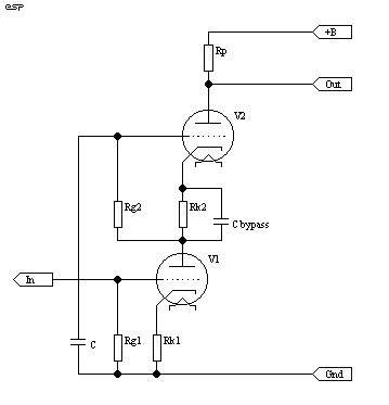
Figure 5.6 - Valve Cascode
Amplifier
As can be seen, the grid of V2 is earthed via the capacitor for all signal frequencies, allowing V2 to operate as common grid. The capacitor (C bypass) is used to ensure that there is no gain lost due to cathode degeneration (local feedback). The cathode of V1 will also be bypassed in many cases, especially where low noise is a primary goal.
The same principles can be applied to FETs or BJTs, and has similar advantages. The capacitance between Drain and gate (or collector and base) is isolated in the same way as with a valve circuit, with the signal being coupled to the source or emitter by the first device. Figure 5.7 shows a composite JFET / BJT cascode circuit, which will have better linearity than a conventional amplifier, and a much better high frequency response.
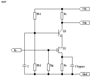
Figure 5.7 - Composite
FET / BJT Cascode Amplifier
This type of circuit is not uncommon in high performance opamps, where very wide bandwidth and good linearity before feedback are required. Cascode circuits are also sometimes seen in solid state power amplifier circuits, where the designer is trying to obtain the maximum possible bandwidth from the amp.
The base of Q2 is grounded to all signal
frequencies, so the stage operates as a common base circuit. Using
a JFET as the input element means that the circuit has a high input impedance,
while the BJT ensures maximum gain. To obtain even more gain, Rc
might be replaced by a current source, in which case the gain from this
single stage can exceed 1000 times, with wide bandwidth and excellent linearity.
Having added Section 5, I think that this article is complete. Until such time as I find (or someone points out) a mistake that I will then have to fix, there will be no further updates.
These are the essential building blocks of nearly all circuits in common use today. There are others (of course) but they are most often combinations of the above - for example, a LTP stage can be built using two cascode circuits, a current source and a current mirror. The resulting circuit looks complex, but is simply a combination of common circuits such as those shown.
Other circuits are modification of the basic stages to exploit what might otherwise be seen as a deficiency - for example circuits that deliberately exploit the temperature dependency of a BJT can be used as high gain thermal sensors, or to stabilise the quiescent current in a power amplifier.
There are also some bizarre combinations possible. A valve and BJT operating in cascode would be interesting, and would no doubt have some desirable characteristics (I haven't seen this particular combination, but there is no reason that it would not work). Likewise, a valve with a transistor current source instead of the load resistor would have far better linearity and more gain than a simple resistor loaded version.
In many cases, ICs are available to accomplish many of the functions described. Opamps are an obvious one, but there are also IC current sources, transistor arrays (ideal for current mirror applications because of the excellent thermal tracking), plus quite a few others.
I hope that I have shed some light on the subject, and that you get some benefit from my musings.
This is the first in what is likely to
become a series of articles describing how things (amplifier things, that
is) work. Should you have any suggestions or comments, please feel
free to send me an e-mail.