
| Elliott Sound Products | Using Current Sources, Sinks & Mirrors In Audio |
Rod Elliott
Last Updated 28 Jan 2000
Integral to most audio amplification systems, the current source and current sink are indispensable. For the purposes of this article, sources and sinks shall be treated as being the same thing - which they are, depending upon how one views the circuit. In essence, the functionality (and purpose) are identical - force the current through another device to be constant, as long as the voltage is within the boundaries of the power supply (less some voltage drop across the source / sink).
Current mirrors have the ability to greatly increase open loop gain and linearity, giving better closed loop performance. This short article looks at the various types, from the theoretical "perfect" device, through various practical examples.
A perfect current source can be constructed very simply, requiring only an infinite voltage and an infinite resistance. Unfortunately, this will also provide an infinite current (which will be infinitely constant), but is (infinitely?) excessive for most applications.
Sorry, I was being facetious, but the principle is nonetheless sound. In reality, a sufficiently high voltage can produce a current through a varying resistance that is essentially constant, provided that the voltage swing on the resistance is a small fraction (<100th) of the supply voltage. This will provide an accuracy of 1% at 100:1 voltage ratio.
This is a method that was common years ago, and I still have (and use) a transistor tester that uses this method to provide a constant base current to the device under test. With a supply voltage of 250V feeding the base-emitter junction (0.65V typically) via switched resistances, the current is not affected at all by any variation in the base-emitter voltage under load.
The principle works well, but no-one wants to have to use such high voltages in equipment these days.
So why mention this method at all? Simply because the operation and characteristics of current sources are not well understood by most non-engineers (and quite a few engineers, too). Figure 1 shows a resistive current source that will maintain the set current of 1mA to an accuracy of within than 1% over the range 0-10V.
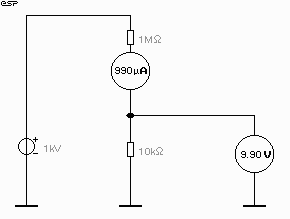
Figure 1 - Simple Resistive
Current Source
The first thing that we need to be aware of is that the impedance is very high, and a perfect current source (as described above) does indeed have an infinite impedance. Although this is impossible to achieve in practice, impedances of many, many megohms are quite possible, and are used regularly in many different circuit types.
If we look at a simple common emitter transistor amplifier (Figure 2), the output impedance is equal to the collector resistance, and the gain is equal to the collector resistance divided by re - the transistor's internal emitter resistance. This is equal to approximately
26 / Ie (mA)
and will naturally vary with the current. Please note that biasing components have been omitted for clarity, but in reality they must be used.
For all examples, a transistor with a current gain of 100 is used and the bias current will be set at exactly 100th of the expected collector current (using a current source, naturally).
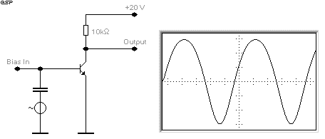
Figure 2 - Simple Common
Emitter Transistor Amplifier
At low output levels, the gain should be 385, but as simulated is actually 397. This is well within the degree of accuracy we want to go to in this article, so practice correlates well with theory (one would hope so, or we would all be in trouble).
As the transistors output voltage increases, the available collector current (and hence emitter current) falls, so re increases (and vice versa). The higher the output voltage (relative to the supply voltage), the less emitter current flows, and the lower the gain becomes. As the transistor turns on (reducing the output voltage), the exact opposite occurs, and the gain rises. This effect is immediately evident in the output waveform, which is distorted. This is shown in the oscilloscope trace in Figure 2, and the distortion is clearly visible, with the tops of the waveform flattened out, and the bottoms "stretched". This is typical of any transistor amplifier operating without feedback, and is also true of valves and FETs.
One method of reducing this distortion is to introduce a resistance into the emitter circuit (local feedback) to reduce the gain and swamp the variations in re. This works, but we still have a relatively low output impedance, and distortion is still evident - although much reduced. This is shown in Figure 3, where a 100 Ohm emitter resistor has been added.
A commonly held belief is that local emitter feedback reduces the output impedance - this is simply not true - the output impedance of a common emitter amplifier is equal to the collector resistance, regardless of emitter degeneration. To reduce the output impedance, it is necessary to apply feedback around the entire circuit - from the output back to the input. The proof of this is outside the scope of this article, but it is nonetheless a fact.
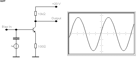
Figure 3 - Common Emitter
Stage With Local Feedback
With all this talk of distortion, I can almost hear all the thermionic valve (tube) enthusiasts cheering "I knew it - and here is the proof I have been looking for!"
Sadly, this is not the case. Valves do exactly the same thing, as do FETs of all types - the mechanism is different in each, but the result is the same. Gain varies with current in all known amplifying devices to a greater or lesser degree, so the principles outlined here are valid for any device. I am staying with transistors because they are the most commonly used of all the devices currently available.
In this case, the gain of the stage works out to be just over 78, and theory would predict a gain of 79, so again the correlation is very good. Remember that with an emitter current of 1.001 mA (collector current plus base current), the value of re is about 26, and this must be added to the external resistance Re.
Since we have determined that the load resistance affects gain, and that variations of collector current (and hence emitter current) affect linearity, if a current source were to be used instead of the 10k resistor, we should get vastly more gain, and the distortion should be negligible.
In reality, this is exactly what will happen, and Figure 4 shows a theoretical current source as the collector load. The current source is set to provide a current of 10 mA as before. No oscilloscope trace is shown, because the linearity is so good that no distortion is visible, and a trace of a sinewave gets tedious after a while.
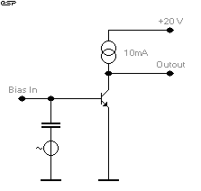
Figure 4 - Use of Current
Source as Load
Figure 4 shows the circuit, which (theoretically) has a gain of about 20,000,000 (and no, there are not too many zeros, it really is 20 Million). Naturally, real life will reduce this considerably - even using a 10M Ohm oscilloscope probe will cause a dramatic loss (down to about 390,000 in fact). In reality, the gain of this circuit is actually infinite, but the "meters" I used in the simulation are "only" 1G Ohm each, which reduces the gain.
Figure 5 shows the same circuit with a real current source, and the gain from this (again, the transistors all have an Hfe of 100) is still quite astonishing. We still manage a gain of 19 Million (bearing in mind the meter load, which reduces the gain).
This form of circuit can no longer be biased using a simple current source, because the circuit gain is so high that even the smallest variation in transistor Hfe, or the tiniest variation in a resistor value will cause the output to "go to ground" or sit at the supply voltage. Consequently, an opamp has been added to apply bias, otherwise the circuit is almost impossible to stabilise. The use of a bias servo in this manner is not too common, but I have seen it used in a number of applications. Care needs to be taken to ensure that a low frequency phase shift oscillator is not created if you want to experiment with this idea.
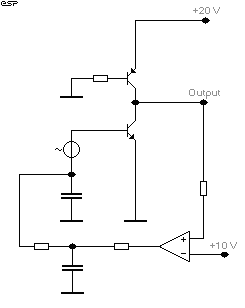
Figure 5 - Real-Life
Current Source Load With Bias Servo
For a current source of this type, the current is equal to
I = (( V - 0.65 ) / R ) * Hfe
The current source shown is workable, but is highly dependent upon the gain of the transistor, and the supply voltage. Now that the basic principles have been examined, we shall look at some real current sources (or sinks, depending on how you look at it).
Where I is the current, V is the supply voltage, 0.65 is the emitter-base voltage (typical), R is the base resistor and Hfe is the forward current gain of the transistor.
The "classic" current source is shown in Figure 6, and is reasonably stable with transistor gains and temperature. In audio work, absolute stability is not really necessary, since the feedback loop is used to ensure that bias voltages are maintained at the correct value. In some cases a servo circuit may be used (as shown in Figures 6 and 7), but this is not really necessary in the majority of cases.
The circuit shown uses the diode stabilised base voltage to maintain a constant voltage across the emitter resistor. As always, a constant voltage across a resistor means that the current is also constant. The output current of this source is calculated from
I = 0.65 / RE
Where RE is the total emitter resistance - the internal re of the transistor plus the external resistance Re. The diode current should be a minimum of 10 times the expected base current, but can be up to 100 times as great.
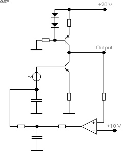
Figure 6 - The "Classic"
Current Source
The gain is relatively unaffected by the change in the configuration of the current source, and the next variation (which is preferred by many designers - including me) has no significant effect either.
In any of the above cases, the inclusion of an emitter resistor (100 Ohms - as shown in Figure 6) reduces the gain to about 3.75 Million - this is still an outstanding amount of gain from a single transistor!
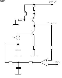
Figure 7 - The Preferred
Current Source
This current source is probably one of the most commonly used, and has excellent stability, especially if the two transistors are thermally bonded. This is not needed for most applications, since as mentioned previously, absolute current accuracy / stability is not (or should not) be a requirement for an audio amplifier.
This is a very simple circuit, but will give excellent results wherever it is used. Current is calculated by
I = 0.65 / Re
In this case, the internal emitter resistance is not an issue, since the second transistor allows only that exact amount of base current for the current source to develop 0.65 Volt across the resistor. Should the current try to increase, the second transistor simply turns on harder, and steals more of the base current. The current through this second transistor should be at least 10 times as great as the expected base current of the current source.
With all the circuits shown, output impedance is very high, and by my tests, is about 500 Megohms (this happens to the the combined resistance of the two meters I used for monitoring, so the actual amplifier output impedance is effectively infinite. Inclusion of the emitter resistor (providing local feedback) has no effect whatsoever on the impedance (contrary to popular belief), but simply reduces the gain.
The final (and least understood) of all the current sources is the so-called "bootstrap" amplifier. While not as good as a true current source, its performance is still very good, and in the example shown in Figure 8 manages to provide a gain of 8,860. Bear in mind that this is at a current of only 1mA (the others all used 10mA), so the gain must be reduced somewhat. However, this circuit is not in the same league as the gain of millions from the current source, but in real terms this is more than enough for the Class-A amplifier / driver stage of a power amplifier.
There are some advantages and disadvantages to this circuit, and it is dependent on the application whether it will be suitable. Where a true current source has the same (more or less) impedance at all frequencies right down to DC, the bootstrap circuit has a low frequency cut-off point determined by the resistance and capacitance used. This makes DC biasing easier (since the gain is quite low at DC), but since it reduces gain (and global feedback) at DC, there may be more DC offset at the amplifier's output as a result.
Distortion will also increase at very low frequencies, since the constant voltage across resistor R2 will not be maintained as phase shift (and LF rolloff) start to take their toll.
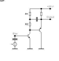
Figure 8 - Bootstrap
Current Source
Since it is so misunderstood, it is worth a few words of explanation. R1 and R2 supply a nominal current of 1 mA (resistors are 5k each). Under normal (i.e. quiescent) conditions, there will be 5 Volts across each resistor. As the output varies, the capacitor couples the output signal back to the centre tap of the two resistors, and if the emitter follower were a perfect buffer amplifier, this would exactly equal the input. As a result, the voltage across R2 is kept constant - if the voltage across a resistor is constant, then it follows that the current through the resistor must also be constant. The current through R1 varies considerably, but R2 maintains a constant current over the full output operating range.
Small differences in voltage (due to the loss through the emitter follower) or in phase (due to the capacitive reactance starting to become significant with decreasing frequency) both cause the bootstrap current source to reduce its effectiveness, so impedance and gain drop, and distortion increases. In a well designed circuit, these effects are minimal at all normal operating frequencies, but cannot be discounted.
Now that we have looked at the various types of current source (there are many more, but the others will not be examined here), we can examine where they are best used, and why.
I am mainly interested in audio amplification, and will therefore concentrate on this aspect of the use of current sources and mirrors. There are naturally countless other applications, but I will leave it to the reader's imagination to explore the additional uses.
One of the most irksome loads for any amplifier is one that has inherent non-linearities, and the output stage of an audio amp definitely fits this description. Consider the worst case, where there is no forward bias applied to the output devices, which are operating in Class-B. The global feedback in an amplifier is generally considered to the be main saviour, by reducing the distortion components by using the input stage as an error amplifier.
This is actually only a small part of the story - a properly designed Class-A amplifier will have both high gain and high output impedance, both of which are useful in reducing the otherwise inevitable crossover distortion. Consider Figure 9a and 9b, showing the same output stage delivering the same peak output voltage to the same resistance.
The first is using a low impedance amplifier (an opamp) with unity gain as shown, but will normally be adjusted to give the required output, while the second uses a high impedance source having a high gain and impedance, but still providing the same output voltage.
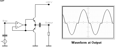
Figure 9a - Use Of A
Voltage Source Driving an Unbiased Output Stage
The load for each amplifier is 100 Ohms, and it is clear from the first figure (9a) that crossover distortion is gross. Figure 9b shows how the high impedance drive to the output stage overcomes the crossover distortion - the output waveform is not shown, because there is virtually no distortion visible in the oscilloscope trace, so it looks just like a sinewave.
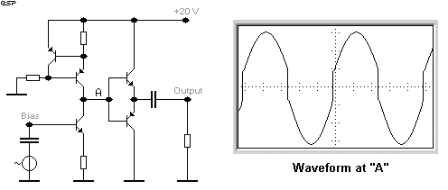
Figure 9b - Use Of A
Current Source Driving an Unbiased Output Stage
Remember that this is with no feedback whatsoever - the addition of feedback will reduce the distortion even more - as will some biasing on the output stage - neither of these were included to show the effect more clearly. Note that the settings on the oscilloscope were not changed between these simulations, to ensure that the full effect was not obscured (or accentuated) for each example.
The inescapable conclusion is that the high impedance drive will greatly assist in overcoming non-linearities in the output stage, even those as nasty as a completely unbiased complementary pair as shown. Naturally other non-linearities are also negated (to some degree) by these techniques, which are pretty much universal in modern amplifier designs.
None of the above should be taken to mean that we no longer need negative feedback - the idea is to make the amplifier as linear as possible before feedback is added. This makes a good amp better - feedback will never make a bad amp good !
The next item is current mirrors, another little understood circuit. These are extremely useful in amplifier design, and in this section I will show where they can be used, and the benefits that can be obtained.
The basic current mirror is shown in Figure 10, and it can be seen that whatever current is injected into the left side is mirrored, and the right hand side is a constant current source (sink) reflecting the injected current. Should the input current at change, so will the output current, but it will remain constant, regardless of the actual voltage (provided it remains within the supply limits of course).
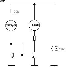
Figure 10 - A Basic Current
Mirror
The problem with this circuit is that the current in the two halves is different - the mirrored current is too low, differing by 19 uA (it is actually 20 uA, but the simulator's accuracy is not great enough to show this). If we check, we will find that the emitter currents of both transistors are identical, so the 20 uA that "disappeared" is the base current that must be supplied to each transistor (10 uA each).
Adding emitter resistors does absolutely nothing to alleviate this, but is useful if the transistors are not matched. Even then the resistors do not really do a lot of good, unless the voltage developed across them is significant (at least 100 mV, and preferably more) but it helps a little bit.
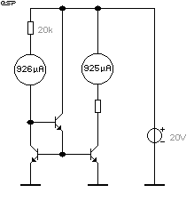
Figure 11 - Buffered
Current Mirror
A better solution is to use a buffer as shown in Figure 11. This removes the base current component of the error, and makes the current mirror matching a lot better. This simple addition has reduced the error dramatically, and now all we have to do is find a use for the circuit.
Consider the differential pair (aka long tailed pair or LTP). Most of the time, we are losing half the gain of the circuit, since the output is taken from only one collector as shown in Figure 12. This configuration also suffers from linearity problems, unless the output is current only - as is the case when driving the base of a transistor (this is shown below).
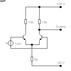
Figure 12 - The Long
Tailed Pair As A Voltage Amplifier
The circuit as shown (without the essential biasing components, which were omitted for clarity) has a voltage gain of 315 (again using transistors with a Hfe of 100), and is quite linear at low output voltages. The linearity will suffer badly as the level increases, and even with the +/-20 volt supplies used is not satisfactory as a voltage amp for outputs greater than about 1.5 Volts RMS (this is at an input voltage of 5 mV).
Using a current source / sink in the "tail" is very common in amplifier circuits, and this variant is shown below. It is commonly (but entirely mistakenly) assumed that this increases the gain, but the real purpose is to improve the common mode capability of the circuit. Common mode signals are those that are applied to both inputs in the same polarity, and are generally required to be rejected. Using a simple resistive tail severely limits the common mode voltage that can be accommodated before severe distortion occurs, and indeed renders the common mode rejection of the circuit almost useless.
In the example above, the common mode rejection is only 1.8 dB but with a current sink tail the rejection is so good that the simulator cannot measure it. In reality this will rarely be the case, but in most amplifier circuits common mode signals (of the undesirable kind) are not an issue if the input stage is properly designed.
If a current mirror is used as the load, gain is increased by a very useful amount, and Figure 13 shows the arrangement used. The stage gain is now over 2,000 and the use of a current sink as the tail has only a marginal effect (provided that the current is maintained at 4 mA). This circuit is shown in Figure 13, and although useful in certain applications, it is not suitable to drive the output stage of a power amplifier.
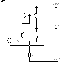
Figure 13 - Using A Current
Mirror The LTP Load
If we really wanted to get silly (and I have seen it done), we can put all the bits together in one place, and finish up with an input stage + Class-A driver, with a total gain of a little over 400,000 (based on 100k feedback loading). This will increase dramatically when the output is buffered, but because of the extremely high impedance, suffers when loaded even with 100k. The buffered current mirror does not help the gain, but reduces output offset. The complete circuit is shown in Figure 14, and is a useful example of the techniques discussed in this article.
As we discovered earlier, extremely high output impedance is not a bad thing for this type of application, because the gain can be kept to a manageable level, but still have the necessary reserve to overcome output stage non-linearity before the application of global feedback.
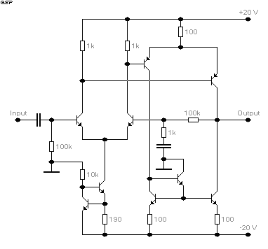
Figure 14 - Combination
LTPs and Current Mirror
This circuit uses an input LTP that drives a secondary LTP as the Class-A amplification stage. The load for this second LTP is a current mirror, and this arrangement has excellent linearity. I suspect that it could be a cow to stabilise in a real amplifier circuit, and quite frankly, I do not see any reason to go this far. One amplifier I have seen using this arrangement was a MOSFET type, and given the inherent non-lineararities of MOSFETs the additional gain is useful. Initial measurements on the MOSFET amp show that stability is not as good as I would like to see (there are traces of oscillation at some output levels), but overall stability seems to be acceptable. I expect that the wide bandwith of the MOSFET output devices might make this arrangement a little more tractable than would be the case with bipolar transistors.
At this stage, I suspect that I have either cleared up some degree of confusion, or created even more. There are so may choices, and so many reasons to use (or not use) any one of them. This article is meant only to describe and explain - you can see where my own preferences lie from the circuits published in the projects pages. I happen to be a strong supporter of the KIS principle (keep it simple), and in my own designs have not found it necessary to make the circuit any more complex than is needed to make it work and provide good distortion figures. Listening tests bear this out, and IMHO I do not believe that the difference between a highly complex amp and a simple one (provided that both are well designed) is audible under any listening condition.
This being the case, I cannot think of any good reason to go for the complex solution, especially since it will almost certainly be much harder to stabilise (I happen to think that this is extremely important), and will use more parts. Granted that the additional cost is minimal in the greater scheme of things, but sound for sound, simple and reliable has to win out.
As a final point, with the LTP configuration and current mirrors, it is often beneficial to match the transistors, so they have gains that are approximately equal, and emitter-base voltages that are as closely matched as possible. It is also useful with both of these configurations and two transistor current sources to thermally bond the two transistors to prevent mismatch due to thermal effects.
Remember that the emitter-base voltage
of a transistor falls at a rate of 2mV per degree Celcius, so even a small
temperature difference will change the DC offset performance quite dramatically.
For more information on the design of amplifier stages, please refer to the Amplifier Design page.