| This version reflects the comments of the core participants as reviewed and incorporated in accordance with CORD's FIPSE-supported Curriculum Morphing Project. | |||||||||||||||
MODULE 4-6 General comments of John Simcik (1) A laser diode, or semiconductor laser, operates similarly to an ordinary forward-biased diode. They are very reliable devices that may have long lifetimes if treated properly. The power source for a laser diode is a simple constant-current supply. Standard laboratory DC supplies are not stable enough. A laser diode supply typically will consist of a slow starter circuit, current regulation, transient suppression, and automatic optical power control.

When you complete this unit, you will be able to: 1. Using terms similar to those in the text, describe various types of laser diode structures and their relationships. When applicable, explain advantages and disadvantages of each structure. 2. Draw a typical curve that shows output power versus forward current. Label the threshold current, operating-current region, saturation point, and catastrophic damage point. 3. Explain the effects of static electricity on laser diodes and describe procedures for establishing a static-free work environment. 4. Identify sources of electrical transients during operation of a laser diode. 5. Describe methods for transient suppression in laser diode power supplies. 6. Draw a block diagram of a simple laser diode power supply, for both continuous operation and pulsed operation. Explain the function of the major components. 7. Explain appropriate mounting and cooling techniques for continuous and pulsed laser diode operation. Draw a typical set of curves that shows how output changes with temperature. 8. List laser diode failure mechanisms and their causes. 9. Describe proper procedures for turning on and off a continuous laser diode, so as to minimize current transients. 10. Exhibit proper soldering techniques for a laser diode. 11. Construct a power supply for a laser diode, incorporating an automatic current control. 12. Measure operating characteristics for a laser diode, including threshold current, output power versus current, and slope efficiency.
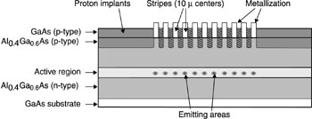
(2) Semiconductor laser diodes represent a class of lasers much different from the gas and solid-state lasers that we have been describing in earlier modules. A semiconductor laser uses a small chip of semiconducting material as the active medium. The most common semiconductor laser material is the alloy aluminum gallium arsenide. We shall return later to a discussion of the materials commonly used for semiconductor lasers. (3) The development of high power diode laser arrays has been an important recent development in diode laser technology. Such arrays offer high radiance diode sources suitable for applications like materials processing and pumping of solid state lasers. An array is often fabricated as a bar with a number of stripe laser diode sources. The stripes are defined by proton implantation, which increases the electrical resistivity of the regions between the emitting areas. There is sufficient coupling of light between the stripes that the entire device acts as a single laser. These devices are capable of emission of many watts of optical power. (4) Such lasers are usually available as bar structures, typically on centimeter long. A single commercially available 1-cm bar can emit up to tens of watts of power in continuous operation and research models have emitted models have emitted hundreds of watts. (5) A number of bars may be stacked to form two dimensional arrays. These arrays are expensive, but represent an important and rapidly developing aspect of semiconductor laser technology. Commercial models are available with up to 50 linear arrays in the stack and are capable of emitting kilowatts of output power. (6) In size and appearance, the semiconductor laser is similar to a transistor or to a semiconductor diode. Thus its properties and its power-supply requirements are quite different from the devices that were discussed in Modules 4-2 through 4-5. In contrast to those lasers, the voltages tend to be very low, a few volts instead of kilovolts. (7) In this discussion, it is assumed that the student is familiar with basic semiconductor terminology, including terms such as conduction and valence bands, energy band gap and p- and n-type semiconductor materials. If this is not the case, the student should refer to any standard text on solid-state physics. (8) The laser operation occurs at a p-n junction, that is the boundary region between p-type and n-type materials. Such a junction can serve as a rectifying diode for electrical circuits, but it is also the critical region for laser operation. The energy-level diagram near a p-n junction is shown in Figure 1. In the neighborhood of the junction, the energy bands undergo a shift as indicated. An energy barrier restricts electrons in the conduction band from flowing to the right or holes in the valence band from flowing to the left. Thus the junction has electrical rectification properties.
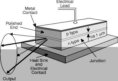
Fig. 1 (9) The left portion of the figure shows the situation with no voltage applied. The electrons to the left of the junction and the holes to the right of the junction are separated. The right portion of the figure shows the situation when a forward-bias voltage is applied to the junction. The barrier height is reduced and some of the electrons in the conduction band will overlap some of the holes in the valence band. Thus there are filled states lying at an energy higher than empty states, in other words a population inversion, the necessary condition for laser operation. (10) In this situation, radiative recombination of the holes and electrons can occur. Electrons fall across the energy gap and recombine with holes. The energy difference is emitted as light, indicated as photons of energy, hn in the figure. Stimulated emission can occur and the junction region can act as a laser. (11) The thickness of the junction region is small, typically around one micrometer. Thus, light traveling in the plane of the junction is amplified more than light perpendicular to it and the laser emission is parallel to the plane of the junction. (12) Because, in operation, electrons are injected into the device from the (13) The laser commonly takes the form of a rectangular parallelepiped as illustrated in Figure 2. The dimensions typically are a few hundred micrometers, up to perhaps one millimeter. The junction is a plane within the structure. Two of the sides perpendicular to the junction are purposely roughened so as to reduce their reflectivity. The other two sides are made optically flat and parallel, by either cleaving or polishing. These two surfaces form the mirrors for the laser cavity. The reflectivity of the air-semiconductor interface is high enough that no other mirrors are needed, although sometimes one of the reflecting surfaces may be coated to increase the reflectivity and to enhance laser operation. The provisions for electrical contacts and for heat sinking also are illustrated.
Fig. 2 (14) The structure shown in Figure 2 is the original historical structure, consisting simply of a junction between p- and n-type layers of the same material. Modern semiconductor lasers contain many layers of material of varying composition, as we shall describe later. (15) For the device to operate as a laser, the population inversion must be high enough so that optical gain exceeds loss. The current through the junction must exceed a minimum threshold value. It must provide enough holes and electrons so that the radiation generated by their recombination exceeds the losses. Losses arise from several causes, including spreading of light out of the active region, transmission of light through the mirrors, and absorption of light by free carriers in the junction. (16) Figure 3 shows the output characteristics of a laser diode as a function of input current. At low values of the input, the device acts as a light-emitting diode (LED), producing a relatively small amount of incoherent light. At a threshold value, where the population inversion is large enough so that gain by stimulated emission can overcome the losses, the laser threshold is reached. As current increases above the threshold value, the light output increases much more rapidly than in the LED region. The light is now coherent laser light. Ideally, the light output should increase linearly with current, as shown in the figure.
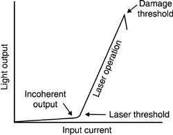
Fig. 3 (17) One defines a slope efficiency to characterize the laser diode output in this region. The slope efficiency is defined as the increase in optical output power divided by the increase in electrical input power. The definition applies only to the region where the output is increasing linearly. It is an important figure of merit that is used to characterize the laser performance. Diode lasers with slope efficiencies around 30% are available. (18) As a specific example, let us consider the Mitsubishi ML4405 laser diode, operating at 25° C at a voltage near 1.8 volts. As the current increases from 35 to 45 milliamperes, the voltage changes very little, but the light output increases from 1.1 to 4.1 milliwatts. The slope efficiency is then: (4.1 - 1.1) ´ 10–3/ 1.8 ´ (45 - 35) ´ 10–3 = 0.167 = 17% (19) Figure 3 also shows the existence of a damage threshold, a value of the input current at which catastrophic optical damage (COD) occurs. Above this threshold, permanent damage occurs and the light output drops rapidly with further increase in current. We shall discuss COD in more detail later. For now we simply note the existence of a damage threshold, which should not be exceeded. (20) In some cases, the curve of output power as a function of input current may show kinks, as indicated in Figure 4. This is generally an undesirable situation, which reduces the stability of the device and which may disqualify it from many applications. The concept of slope efficiency is not valid if kinks are present. The manufacturers of laser diodes have worked diligently to produce stable devices that do not exhibit the behavior illustrated in this figure.
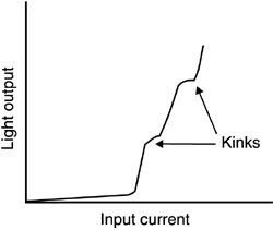
Fig. 4 (21) The output characteristics of diode lasers are strongly dependent on the operating temperature. Figure 5 shows how the current-output curve changes with temperature for typical laser diodes. As temperature increases, the threshold current increases. At a given value of current above threshold, the output decreases with increasing temperature. Usually the manufacturer will specify some maximum operating temperature for a laser diode.
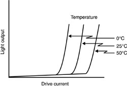
Fig. 5 (22) The threshold current depends on temperature in an exponential fashion, according to the equation: It(T2) = It(T1) ´ exp[(T2 – T1)/T0] Equation 1 where It(T2) and It(T1) are the threshold currents at temperatures T1 and T2 respectively, and T0 is a scale factor with a typical value around 150 K. As an example, if T1 = 0° C and T2 = 30° C, the threshold current will be about 22% higher at the higher temperature. (23) The beam emitted from a semiconductor laser typically has an elliptical spatial profile, as illustrated in Figure 6. The profile is caused by diffraction. In the dirgction perpendicular to the junction, the beam is confined by the narrow junction, typically of width around one micrometer. The beam in that direction is spread by diffraction to an angle often as large as several tens of degrees. In the direction parallel to the junction, the beam is not confined so stringently and spreads less, perhaps to around ten degrees or so. The result is a fan-shaped beam, as indicated in the figure. The beam is said to be astigmatic.
Fig. 6 (24) The astigmatism results from the separation between the apparent sources of the emission for the radiation parallel and perpendicular to the junction. The amount of astigmatism is specified as the distance equal to the numerical value of the separation. A typical value for the astigmatism may be around 10 micrometers. (25) The astigmatism may be corrected, at least partially, by the use of cylindrical lenses to form a circular profile. Still the beam divergence is substantially larger than what one is accustomed to with lasers. Typical gas lasers, with a diffraction-limited beam emerging from an aperture around 1.5 millimeters in diameter usually have a circular beam with divergence of a few tenths of a degree. Thus semiconductor diode lasers typically have much lower radiance than other types of lasers. Also, their radiation cannot be focused so well as the light from better-collimated lasers. (26) Laser diodes offer many advantages, including small size, light weight, low power consumption, and high efficiency. They have become widely used as light sources for a wide variety of applications, including compact disk players, printers, magneto-optic data storage, and optical-fiber telecommunications.
Semiconductor Laser Materials (27) Most semiconductor laser materials are fabricated from so-called
III-V compounds, that is compounds formed by elements from column III and column V of
the periodic table. An example is gallium arsenide, which in fact was the first
semiconductor laser material. The original semiconductor lasers were fabricated from
crystals containing a junction between p- and n-type gallium arsenide. Such lasers have
been superseded by structures formed of alloys that contain three or four elements from
columns III and V of the periodic table. These alloys are called ternary or quaternary
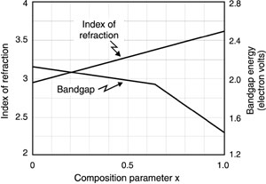
compound semiconductors, respectively. Examples are (28) The properties of the material also vary continuously as x and y vary, Figure 7 shows how the bandgap and the index of refraction vary in the Al1–xGaxAs system as x changes.
Fig. 7 (29) The most common of the semiconductor lasers is the Al1–xGaxAs laser. The output wavelength varies with x and commercial devices are available with outputs ranging from about 780 to 880 nm. They are used for applications including optical disks, optical-fiber telecommunications, and laser printers. (30) Another common semiconductor laser material is the quaternary alloy (31) Another important type is AlxGayIn1–x–yP, in which Al, Ga, and In are all column-III elements whose total must equal the number of phosphorous atoms. This alloy is notable for operation in the red portion of the visible spectrum, at wavelengths from 630 to 680 nm. It is finding application as a replacement for helium-neon lasers in some of their applications. (32) Table 1 summarizes these three most important types of semiconductor laser materials.
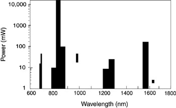
(33) All these lasers are commercially available from a number of sources. Figure 8 illustrates commercial availability of the most common semiconductor lasers, showing the ranges of wavelength and output power available. The choices have been driven largely by the needs of optical-fiber telecommunication, which accounts for many of the uses of devices in the 830-, 1300-, and 1550-nm regions. The cost for relatively low-power (a few milliwatts) laser devices in the 800-nm region can be quite low, perhaps $5-10 in quantity. The price increases rapidly as output power increases.
Fig. 8 (34) A number of other semiconductor laser types is available, based on II-VI compounds, such as PbS1–xSex. These devices operate in the long-wavelength infrared region, require cryogenic operation, are very costly, and are far less common than the other laser types described above.
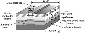
Structures of Laser Diodes (35) We have so far described the most simple and now obsolete structure of semiconductor diode laser, a rectangular block of material with a p-type region and an n-type region and a p- n junction plane parallel to one of the surfaces, as indicated in Figure 2. Modern diode lasers are formed of structures that contain several thin layers of material of varying composition. One example, out of many possible, of the types of layers that are possible, is shown in Figure 9. Figure 9 illustrates the complexity of the structures that have been developed. The material is grown in thin layers, typically with thickness of the order of one or a few micrometers, starting on a substrate of semiconductor material. The growth is accomplished by carefully controlled epitaxial growth techniques, such as vapor phase epitaxy. Such growth techniques deposit very thin layers of material of specified composition as single crystalline layers of high perfection.
Fig. 9 (36) The structures may contain several layers of material of varying composition and doping levels. At some position, a p-n junction region is formed. The junction region is the location where the laser operation occurs. The notations p+ and n+ refer to heavily doped conductive regions of p- and n-type material, respectively. We shall describe the functions of the regions of varying composition below. The figure also indicates some other features, such as the use of proton-bombarded areas that have low electrical conductivity. The proton-bombarded areas essentially form a stripe that confines the current and defines the area where laser operation will occur. The incorporation of a stripe, either in this fashion or by selective metallization of the surface so that the electrical contact is in the form of a stripe, is a very common feature for semiconductor lasers. Figure 10 shows the incorporation of a stripe by means of selective insulator and metallization layers. The current flows only in the region where the metallization contacts the semiconductor.
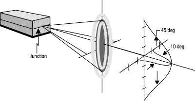
Fig. 10 (37) Now let us consider the functions of the different layers of semiconductor materials, as illustrated in Figures 9 and 10. The heavily doped layers are electrically conducting, facilitating making the electrical contacts. The sequence of layers AlGaAs-GaAs-AlGaAs forms what is called a double heterostructure, in which there are two changes of composition of the material as one goes through the active light-emitting region. (38) To understand the function of the double heterostructure, let us first consider the earliest devices, as illustrated in Figure 2, in which the junction was formed by a junction between p- and n-type GaAs. This was a material with a single composition; the junction was called a homojunction (also called a homostructure). Figure 11 shows a homojunction structure and how the index of refraction of the material changed as one went through it. It was called a homojunction because the material on each side of the junction had the same composition. The variation in doping provided a small step in the index of refraction, as indicated on the right side of the figure. This tended to provide some confinement of light in the region of the junction, because of total internal reflection. However, the step in the index of refraction was small and the confinement was relatively poor. The losses due to spreading of light out of the active region were large, so that the drive currents had to be large, and these devices were short-lived and subject to damage. Homojunction diode lasers are now extinct.
Fig. 11 (39) The use of a single heterojunction (also called a single heterostructure) as shown in the middle portion of the figure provided better confinement. In this structure, there is one change in composition of the material as one goes through the junction, so the device is called a single heterojunction. The structure provides a large change in index of refraction, according to the data shown in Figure 7. The heterostructure reduces the light that leaks into the p+ region because of waveguiding effects. This in turn leads to lower losses, lower current requirements, reduced damage, and longer lifetime for the diodes. Single heterostructure diode lasers are still in use, but have largely been replaced by double heterostructure devices. (40) The bottom of the figure shows the double heterojunction (or double heterostructure), so called because there are two changes in the composition of the material as one goes through the junction. This confines the light from both sides by waveguiding effects and reduces the current requirements even further. Double-heterostructure (also called double heterojunction) devices are now widely used, having mostly replaced the other types. They offer the possibility of very long lifetime (many tens of thousands of hours) if used properly. (41) There is an extremely wide variation in the structures of semiconductor diode lasers and in the way the layers are actually configured. It is impossible to cover them all here. Figure 12 represents a simplified classification scheme showing some of the major subdivisions of diode lasers and their relationship.
Fig. 12 (42) The first major division is into edge-emitting and surface-emitting devices. So far we have described only edge-emitting structures. They are of the form shown in Figure 9, in which the light emerges from the edge of the device, where the junction intersects the surface. The light emerges in the plane of the junction. The configuration is simple and easy to fabricate. Most diode lasers are edge-emitters. But they do suffer from the drawback that the volume of material that can contribute to the laser emission is limited and they are difficult to package as two-dimensional arrays. (43) In recent years considerable research activity has been aimed at development of surface-emitting diodes, in which the light emerges from the surface of the chip rather than from the edge. This feature is attractive because devices could be packed densely on a sgmiconductor wafer and it would be possible to fabricate two-dimensional arrays easily. Some commercial models of surface-emitting diode lasers have become available and it seems certain that they will continue to develop in the future. Still, edge-emitting lasers are far more common and the remainder of this discussion will concern only edge-emitting devices. (44) The edge-emitting devices may be divided into homojunctions, single heterojunctions, and double heterojunctions, concepts that have been discussed above. The homojunctions are no longer used and double heterojunctions dominate most applications. (45) These devices may have a stripe geometry, in which the gain region is confined to a narrow stripe region, as we have described. Without a stripe, the laser light will emerge all the way across the width of the diode. This is denoted in the figure as "broad area." It allows the generation of higher power, because a larger volume of oaterial may contribute to the laser operation, but it leads to greater astigmatism, because the limiting apertures in the directions parallel and perpendicular to the junction have much different values. (46) Now let us consider methods for defining the stripe geometry. Confining the laser operation within a stripe region may be accomplished by gain-guiding or by index-guiding. Both methods confine the light so as to reduce the loss due to beam spreading. This in turn reduces the current requirements for laser operation and thus allows operation well away from the damage threshold. The use of some method of confining the light is essential to producing long-lived laser diodes. It also leads to limiting apertures that are more nearly equal in the directions parallel and perpendicular to the junction, and thus reduces astigmatism. (47) Index-guided lasers employ steps in the index of refraction both parallel and perpendicular to the junction to confine the light. We already have discussed confinement perpendicular to the junction in the discussion of heterojunctions. Index-guided lasers also have a change in the index of refraction in the plane of the junction to reduce spreading of light within the junction. Figure 13 shows one geometry as an example, out of many possible variations.
Fig. 13 (48) Gain-guiding employs composition changes and refractive index changes in the direction perpendicular to the junction to confine the light, just as index-guided devices do. But the confinement of light in the plane of the junction is accomplished by refractive index changes that result from higher charge carrier density in the region where gain is high. The use of stripe geometry helps the gain-guiding by confining the carriers and the gain region. Figures 9 and 10 have shown two examples of gain-guided structures, one in which the gain is confined by ion implantation to reduce the electrical conductivity in selected regions and the other in which the current is confined by selective contacting of the metallization to the semiconductor. (49) Gain-guided lasers are easier to fabricate than index-guided lasers, but they have weaker confinement, which leads to somewhat poorer beam quality and stability. Gain-guided devices also have somewhat larger astigmatism than index-guided devices. These factors may restrict the use of gain-guided devices for some applications where beam quality is important, but for many applications gain-guided diode lasers are suitable. (50) To summarize the differences between gain-guided and index-guided structures, index-guided devices have small astigmatism, lower threshold current, and usually a relatively clean output beam, often a single transverse mode, but are more complex and costly to fabricate. Gain-guided devices have larger astigmatism, higher threshhold current, and usually multiple transverse modes in the output, but have a more simple fabrication process and thus are less expensive. (51) Before concluding the discussion of laser diode structures, it is worth mentioning two additional types of structures that have developed rapidly in recent years. These are quantum well devices and high-power laser diode arrays. A quantum well is a very thin layer of semiconductor material between two layers with larger values of bandgap. If the layer is thin enough, 20 nm or less, quantum mechanical properties of electrons become important. This changes the energy-level structure of the material. (52) Quantum well devices may incorporate a single quantum well or multiple quantum wells, with a number of alternating thin layers of high-bandgap and low-bandgap material. The use of quantum wells in laser devices allows the material grower to optimize the properties of the material for the specific application. Quantum well devices offer lower threshold current and higher output power than devices without quantum wells. (53) The development of quantum-well diode lasers has been the topic of intense research for a number of years and some quantum-well lasers are becoming commercially available. (54) The development of high-power linear arrays offers high-radiance diode sources suitable for applications like pumping solid-state lasers. The array is fabricated as a bar with a number of stripe laser sources. A typical arrangement is shown in Figure 14. The stripes are defined by proton implantation, which increases the electrical resistivity of the regions between the emitting areas. There is sufficient coupling of light between the stripes that the entire device acts as a single laser. These devices are capable of emission of many watts of optical power.
Fig. 14 (55) Such lasers are usually available as bar structures, typically one centimeter long. A single commercially available 1-cm bar can emit 20 watts of power, and research models have emitted hundreds of watts. They may be stacked to form two-dimensional arrays. These arrays are still expensive but represent an important and rapidly developing aspect of semiconductor laser technology. (56) In summary, diode laser structures can be extremely diverse. We have covered a few of the major variations in this discussion.
Laser Diode Damage and Lifetime (57) Semiconductor lasers are subject to damage from a number of causes, which include the following:
(58) The most serious degradation involves catastrophic optical damage (COD), which occurs when the laser power at the surface of the laser diode becomes too high, greater than about 106 W/cm2. Absorption of laser light at the surface leads to heating, which in turn increases the absorption further. The result is a feedback process that leads to high temperature and melting of the diode surface and destruction of the laser. (59) As a result of this process, the output power of a laser diode as a function of drive current may appear as was shown in in Figure 3. The output increases with increasing current above some threshold current. When the output becomes too high, COD occurs and the output drops precipitously. The surface damage may prevent laser operation completely, or may allow some operation at reduced power. (60) Even without COD, the output of a semiconductor laser gradually decreases after prolonged operation, probably due to buildup of damage around faults or defects originally present in the material. This gradual aging is manifested by decreasing light output and increased current to maintain a constant light output and possibly by changes in beam profile or wavelength or spectral content of the light. It also may include development of dark-line defects, areas in the active region that do not emit light. (61) The gradual aging can involve operation at excessive temperature or current, but does seem to be associated with defects in the original laser material growth. It can vary widely from one batch of laser diodes to another. (62) If the current is kept reasonably small and the operating temperature is kept low, the lifetime for a semiconductor laser may be quite long, years or even decades. Sometimes manufacturers have claimed, on the basis of accelerated aging tests, that lifetimes could exceed 100 years. (63) The operating lifetime of a laser diode is reduced significantly by operation at elevated temperature. The lifetime is reduced by a factor that varies with absolute temperature T as exp Ea/kT, where Ea is an activation energy, typically around 0.5 to 0.7 eV, and k is Boltzmann’s constant. According to this dependence, an increase in operating temperature of 40 Celsius degrees will decrease the lifetime by a factor around 30. (64) Figure 15 shows some data for typical 5-milliwatt Al1–xGaxAs laser diodes. The figure shows the percentage of laser diodes that have failed as a function of operating time, for various operating temperatures. At 20° C, the mean time before failure is 770,000 hours, but at 70° C, it has fallen to 27,000 hours.
Fig. 15 (65) Static electrical discharges are potentially damaging to semiconductor lasers. The presence of static electricity in the work area will burn out laser diodes easily. Laser diodes are more sensitive to static electricity than other familiar semiconductor devices. Many new users of laser diodes will destroy some number of them before learning to control static electricity. (66) Another hazard to semiconductor diode lasers is excessive voltage, which may arise from power-supply transients. Many power supplies produce voltage spikes during turn-on or turn-off. These voltage spikes may be large enough to cause damage to the semiconductor laser. (67) In practice a large fraction of semiconductor lasers does in fact fail due to "electrocution" in some form, because of electrical transients or because of static electricity. The probability of this happening depends on the skill and experience of the user, and on the particular application. If a semiconductor laser is used by experienced personnel under carefully controlled conditions of temperature and current, it may well last for a very long time. (68) Now we shall consider the methods to reduce damage and extend the lifetime of laser diodes. (69) The most important method available to the user to extend the life of semiconductor lasers is to make sure that the laser is not driven at too high a current. The user should limit the current to the maximum value specified by the manufacturer for the specific laser. The power supply should have current-limiting features that do not allow the safe value of current to be exceeded. (70) The use of drive circuits with automatic power monitoring and control has become common. A photodetector monitors the output of the laser diode and provides feedback to the drive circuit to keep the laser output constant. The design of such circuits will be described in the section on power supplies. (71) Gradual aging cannot be eliminated completely, but its effects can be minimized by keeping the current and the temperature of the diode within reasonable limits. (72) Since unexpected power-supply transients can "electrocute" a semiconductor laser without warning, one should use power supplies specifically designed for use with laser diodes. These power supplies have slow start-up features that reduce initial current transients. During start-up, the leads to the laser diode should first be shorted and the current control should be reduced to a low setting before the power supply is turned on. After turn-on, the short may be removed and the current control then may be raised slowly to the specified value for full laser output. During turn-off this procedure may be reversed. (73) To reduce the possibility of static electrical discharges, the electrical charge should be allowed to bleed off through a high resistance, around 1 megohm. The user should be well grounded through a high resistance (1 MW ). The user should wear a grounded wrist strap and a grounded foot strap when touching semiconductor lasers. The work area also should be grounded, including the use of grounded floor mats and conductive tops for work tables. Shoes should be an antistatic type, i.e., leather rather than rubber or plastic. The laser diodes should be stored in their original antistatic shipping bags when they are not in use. Figure 16 illustrates some of the measures that may be used to combat the effects of static electricity. (John Simcik)
Fig. 16 (74) Proper soldering techniques are also important when attaching the leads of laser diodes. The soldering-iron tip should be grounded. The laser diode should be mounted on a heat sink. Minimum heat should be used. It is generally recommended that the soldering time should be less than five seconds at a temperature less than 250° C. Some laser diode manufacturers include soldering instructions with their diodes. (75) Finally, because the lifetime decreases exponentially with increasing temperature, the laser must be in good thermal contact with a heat sink capable of dissipating the thermal load generated by the laser. We shall discuss this further in the next section.
Mounting and Cooling of Laser Diodes (76) Laser diodes are purchased not as bare semiconductor chips, but mounted in housings that allow easy handling and mounting to heat sinks for heat removal They also incorporate electrical leads attached to the chip. Often the housing is similar to a transistor housing or other integrated circuit package. They usually have provision for direct attachment to a heat sink. A typical view of a packaged semiconductor laser on a mount is shown in Figure 17.
Fig. 17 (77) We have already described the harmful effects of excess temperature, both on laser performance and on lifetime. To dissipate the heat generated by the electrical current, good heat sinking is essential. The heat sink may be simply a flat piece of metal, like copper or aluminum. A sheet with dimensions of 2 ´ 20 ´ 30 mm is adequate for dissipating about 200 milliwatts of electrical power. Commercial heat-sink structures are also available, often with fins to help dissipate the heat. (78) The laser must be mounted intimately to the heat sink, to minimize thermal resistance. It must be remembered that the case temperature, which is what is easily measured, is always lower than the junction temperature, which is what is important. The manufacturers of laser diodes have developed structures with low thermal resistance, to keep this difference small. The thermal resistance is defined as the change in junction temperature per unit change in power. Low values of this parameter are desirable. The thermal resistance of the diode is often in the range from 10 to 50 C° /watt. Some manufacturers specify the value of the thermal resistance of their diodes. (79) Control of the temperature is also necessary to stabilize the wavelength of laser operation. Al1–xGaxAs lasers shift their wavelength of operation at a rate around 0.25- 0.3 nm/C°, with the wavelength increasing as the temperature increases. Thus if a specified operating wavglength is required, the temperature of the diode must be accurately controlled. (80) In many cases, especially when operating at low power, simple air cooling is sufficient. But for higher-power lasers, or when precise control of laser wavelength is required, active cooling is needed. This is usually accomplished with thermoelectric coolers. Thermoelectric coolers employ the so-called Peltier effect. When a current passes through the junction of two different conducting materials, the junction will be heated or cooled. Reversing the direction of the current flow changes the effect from heating to cooling or vice versa. The materials used are usually semiconductors. Thermoelectric coolers are commercially available and represent small, compact devices, which require no water inlets or other fluids. They are very suitable for providing localized cooling for devices like laser diodes. Many manufacturers offer heat sinks, thermoelectric coolers, and thermoelectric cooler drive circuitry that are compatible with commercial laser models. (John Simcik)
Power Supplies for Laser Diodes (81) The input power requirements for semiconductor diode lasers are much more modest than for most lasers. Instead of the kilovolt power supplies encountered with gas and solid-state lasers, diode lasers typically are powered by a few-volt battery. The voltage appearing across typical diode lasers is in the range 1.8 to 2.5 volts. Threshold currents for single Al1–xGaxAs lasers are often in the range 30 to 60 milliamperes. Operating currents for a 10-milliwatt device may be around 80-90 milliamperes. Thus, semiconductor lasers are relatively efficient, much more so than most other laser types, and require very modest voltage, current, and power input. This makes them attractive for many applications. (82) The semiconductor laser is a current-controlled device, rather than a voltage-controlled device. The power supply, or driver, as it is commonly called, must simply furnish a well-regulated and controlled supply of current, often in the range of 100 milliamperes or so. Thus the driver circuit in principle can be as simple as the one shown in Figure 18. This circuit is basically a battery in series with a variable resistor and a switch. The symbol commonly used for a laser diode is indicated. Such a circuit would be suitable for operation of a continuous laser diode. It is extremely simple and would have low noise. It lacks some features that are desired for laser diode operation, including current control and regulation, and limitation of current spikes upon turn-on. Thus, practical laser diode driver circuits usually become more complex than the one shown in Figure 18.
Fig. 18 (83) Ideally what does one desire for a laser diode driver circuit? Important features include:
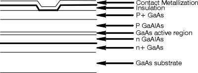
(84) It might seem simple to use a common DC laboratory power supply to drive a semiconductor laser diode. But most DC power supplies are not well suited for driving diode lasers. They lack sufficient stability and may have too-high noise. They frequently have transient current spikes associated with turn-on, spikes that may easily destroy the diode. In addition, it is difficult to modulate the DC supplies. (85) Thus, specialized circuits designed for laser diode operation are usually employed. They take a very wide variety of forms. We shall present a few examples of representative circuits. (86) A relatively simple circuit suitable for driving a continuous unmodulated laser diode is shown in Figure 19. In the use of this circuit, to avoid transients, the laser diode should be shorted with the shorting switch before the power supply is turned on. The voltage should be turned to its minimum value. Then the power supply should be turned on and the current increased slowly until the desired value is reached. To turn off the diode, the procedure should be reversed.
Fig. 19 (87) A relatively simple circuit for driving a pulsed laser diode is shown in Figure 20. The capacitor is charged while the silicon-controlled rectifier is open-circuited, so that the laser diode is not in the circuit. Then the silicon-controlled rectifier is triggered by a voltage pulse. When the silicon-controlled rectifier closes, the capacitor discharges through the path that includes the laser diode. The resistor in series with the discharge (perhaps 2 ohms) limits the current and helps to reduce ringing. The protective diode also helps to suppress ringing.
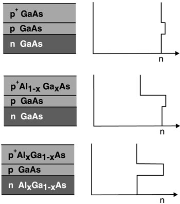
Fig. 20 (88) So far, we have shown only a few very basic circuits. In actual applications, the circuits tend to become more complex and incorporate more specialized features. They also are specific to the particular application. It is not possible to describe all the great variety of drive circuits that have been employed. Rather we shall present a few representative examples. (89) Figure 21 shows a transistor switching circuit developed for optical-fiber telecommunication applications. It is capable of producing pulses as short as 10 ns at a pulse repetition rate above 100 kHz.
Fig. 21 (90) Many drive circuits for laser diode application incorporate so-called "slow starter" circuitry. The function of the slow starter circuit is to bring up the current pulse gradually, so as to avoid potentially damaging transient pulses of current. It also avoids overshoot and ringing of the current as the laser diode is turned on. The slow starter circuits bring up the current over a period around 0.1 second. Any transient spikes have died out by that time. (91) An example of a slow starter circuit is shown in Figure 22. The transistors provide a current shunt for the laser diode until the capacitors charge enough to revgrse-bias the emitter-based junctions. When the power is turned off, the capacitors discharge rapidly so that the circuit returns to its original state.
Fig. 22 (92) The manufacturers of laser diodes offer modules that contain both a laser diode and a photodetector. The purpose is to provide automatic power control (APC). Some of the output of the laser is fed directly to the detector. The APC drive circuit acts as a feedback loop from the output of the detector to the input of the laser diode. It can be useful for providing constant laser output in an environment where the temperature is fluctuating. An example of an APC circuit, driving a module containing both detector and laser diode, is shown in Figure 23.
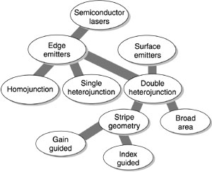
Fig. 23 (93) The use of integrated circuits as drivers can simplify the circuitry. Figure 24 shows a relatively simple circuit incorporating an LM723 IC. This IC incorporates a series pass transistor for current control, an operational amplifier, and a voltage reference. The circuit shown has very low noise. It is suitable for driving continuous laser diodes.
Fig. 24 (94) In addition, laser manufacturers have developed models of integrated circuits specifically to power their laser diodes. The use of a specific driver IC (Sharp IRC302A) to power a laser diode is shown in Figure 25. This example also includes an integrated laser diode/detector with APC.
Fig. 25 (95) Finally, equipment manufacturers now offer complete modular systems of laser drivers, with options for closed-loop thermoelectric coolers, temperature sensors, and controllers. The modules are designed to be compatible with the packages of major diode manufacturers. They incorporate protection against transient spikes and overshoot during turn on. They offer the capability for digital modulation at variable frequency. (96) In summary, laser diode power supplies cover a wide range of complexity and sophistication, ranging from basic battery drive of a continuous diode to advanced circuits designed for specialized applications.
Laser diodes, Sharp LT022 or equivalent Soldering iron Solder and flux Electrical wiring Switch, single-pole, single-throw Voltmeter Ammeter Operational amplifier, JRC2904D or LM2904D Transistors 2SC1815, 2SC2235, and 2SA11660, 1 each Capacitors, 100 m F and 0,068 m F (1 each), 22 m F and 1.5 m F (two each) Potentiometer, 5 kW Resistors, 8.2 kW , 165 kW , 100 W , 2 W , and 3 W (1 each), 2.7 kW (two) Five-volt DC power supply Optical power meter (spectral response compatible with laser diode output) 
(97) First, demonstrate proper procedures for soldering the leads of the laser diode. Solder the leads from the laser diode housing to electrical wiring. Use the procedures suggested by the manufacturer of the laser diode or, if they are not available, follow the guidelines discussed in the text. In this portion of the procedures, you may use a laser diode that has previously been burned out. (98) Next, construct a power supply for driving a laser diode. The power supply will be an operational-amplifier-based supply that offers automatic current control. Fabricate the circuit as shown in Figure 26. Alternatively, if the parts are not available, you may fabricate the circuit shown previously in Figure 19.
Fig. 26 (99) In the circuit in Figure 26, the op amp acts as a high-gain comparator. The 5-kW potentiometer allows setting of a level control. The circuit applies feedback so that the voltage at point A corresponds to the setting of the level control. The circuit then supplies a constant current to the laser diode, according to the setting of the potentiometer. The value of the current is controlled by the setting of the potentiometer, and will remain constant so long as the potentiometer setting is unchanged. The slow-starter portion of the circuit near the left of the figure offers protection against current surges. (100) In operating the laser, observe all the laboratory rules on laser safety and use of protective eyewear. (101) Before turning on the power supply, close the shorting switch and adjust the potentiometer to its minimum setting. Turn on the power supply. Then open the switch and adjust the potentiometer slowly to increase the current. Monitor the current using the ammeter. Be sure to stay below the maximum value of current specified by the manufacturer. When turning off the laser, reverse the procedure. (102) Direct the beam from the laser into the power meter. The distance between the laser and the power meter should be short to ensure that all laser light enters the meter. Gradually increase the current in steps from below the threshold for laser operation to well above the threshold, making sure that the maximum current rating of the diode is not exceeded. At each step, record the output power, the current through the diode, and the voltage across the diode. Plot the output power as a function of the current through the diode. From the plot, identify the threshold current for laser operation. (103) Identify two points on the curve above the laser threshold and in a region where the curve is linear. Calculate the slope efficiency from the equation: Slope Efficiency = 100 ´ (P1 - P2)/(I1V1 - I2V2) where point 1 is considered to be the point with higher output; P1, I1, and V1 are the output power, current, and voltage at point 1; and P2, I2, and V2 are the output power, current, and voltage at point 2. 

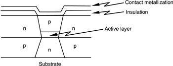
1. Using terms similar to those in the text, describe various types of laser diode structures and their relationships. When applicable, explain advantages and disadvantages of each structure. The description should include edge-emitting devices, surface-emitting devices, homojunctions, single heterojunctions, double heterojunctions, stripe geometry, gain-guided devices, and index-guided devices. 2. Draw a typical curve showing output power versus forward current. Label the threshold current, operating current region, saturation point, and catastrophic damage point. 3. Explain the effects of static electricity on laser diodes and describe procedures for establishing a static-free work environment. 4. Identify sources of electrical transients during operation of a laser diode. 5. Describe methods for transient suppression in laser diode power supplies. 6. Draw a block diagram of a simple laser diode power supply, for both continuous operation and pulsed operation. Explain the function of the major components. 7. Explain appropriate mounting and cooling techniques for continuous and pulsed laser diode operation. Draw a typical set of curves showing how output changes with temperature. 8. List laser diode failure mechanisms and their causes. 9. Describe proper procedures for turning on and off a continuous laser diode, so as to minimize current transients.
Hecht, J. The Laser Guidebook. New York: McGraw-Hill, Inc., 1992. Kapon, E. "Semiconductor Diode Lasers: Theory and Techniques." Handbook of Solid-State Lasers, P. K. Cheo, ed. New York: Marcel Dekker, 1989. Kressel, H., and J. K. Butler. Semiconductor Lasers and Heterojunction LEDs. New York: Academic Press, 1977. Laser Diode Operator’s Manual. San Jose, CA: Spectra Diode Labs, 1989. Laser Diode User’s Manual. Japan: Sharp Corporation (Sharp Electronics Corporation, Camas, WA), 1992. Wieman, C. E,. and L. Hollberg. "Using Diode Lasers for Atomic Physics." Review of Scientific Instruments 62 (January 1991): 1.
|
|||||||||||||||


