Technical Memo
|
|
Warner Instruments Technical Memo |
|
Home Back |
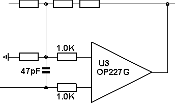
Author: Gene Warner Date: 04/22/95 No of Pages: 5 Re: Measuring Circuit Susceptibility to Cellular Frequencies Background: Over the past two years, or so, there have been intermittent, and sometimes rather vague complaints suggesting that certain products using our standard OP-227 thermocouple measuring circuit were severely affected by security guard walkie-talkies. Assuming walkie-talkies operating in the 27MHz or 50MHz bands (typical), we were not able to duplicate the reported problem. Since the complaints arose from a very small segment of the installed base of products of this type, and usually dissolved as rapidly as they arose, we were inclined to attribute whatever the problem was to local anomalies. t Then, acting on a hunch, we exposed products of this design to near-by cellular telephone transmissions ... and found that this was apparently the nature of the interference giving rise to such complaints. The design of this particular circuit had evolved from all prior experience, and emphasized noise immunity ... and was, in fact, considered to be a very successful design in that respect. However, exposure to nearby cellular activity was not one of the sources of interference anticipated in the design, and these simple tests indicated that, indeed, the circuit seemed to have a particular susceptibility to RFI in this frequency range (approx 800-900MHz). Findings: Initial efforts to determine the cause of this unusual susceptibility and correct it, proved very frustrating. We eventually learned that the problem resulted from a known, but obscure, characteristic of the OP227 op amp (and others) which, in the non-inverting configuration, has a tendency to exhibit an input impedance which has a negative susceptance (reactive conductance) component at some frequency ... usually in the VHF range ... due to the feedback effects of stray circuit capacitance. In practical terms, this means the amplifier's input may exhibit an effective negative resistance at some frequency range, at which it becomes an oscillator! t This has nothing to do with the amplifier's gain bandwidth product. Even if the amplifier is normally very stable, it can become hyper-sensitive to rfi from an external source because of the frequency dependent negative resistance exhibited by the non-inverting input. The simple cure for this condition then suggests itself ... destroy the negative resistance at the non-inverting input by adding some positive resistance. Trials indicated that a wide range of values satisfied this requirement, and a value of 1K was finally selected. To balance the inputs, in recognition of input bias currents, a 1K resistor was inserted at both the inverting, and non-inverting inputs. Adding a 47pF ceramic disc capacitor across the opposite ends of these input compensation resistors also proved beneficial, slightly improving the ability of the circuit to reject rfi at cellular frequencies, and other high frequencies. Design/Engineering Changes: To eliminate cellular/rfi problems, install 1K resistors between pins 10 and 11 of the OP227GN chip and the circuitry originally connected to these pins. Secondarily, connect a 47pF ceramic disc capacitor across the ends of these input compensation resistors, at the nodes connected to the original other circuitry. t
 The existing 1.0uF input compensation capacitor should be removed, and discarded. At the present time, cellular/rfi problems have only been reported in applications involving TempSentry and TempSentry II products. All factory shipments from this date forward (Serial Numbers 1695000, up) will have the above feature factory installed. Field Modifications - TempSentry: Improved immunity to cellular/rfi can be easily and inexpensively added to the installed base of TempSentry (horizontal) units, as follows: t Material Required: CAPACITOR, CERAMIC DISC, 25v 10% 47pF 1 EA
Field Modifications - TempSentry II: Improved immunity to cellular/rfi can be easily and inexpensively added to the installed base of TempSentry II (vertical) units, as follows: Material Required: CAPACITOR, CERAMIC DISC, 25v 10% 47pF 1 EA
For those in possession of installed units and not desiring to install this modification locally, factory service is available. This modification will be installed without charge in any unit presented at the factory for that purpose. Units may be shipped to the above address. Prior authorization is not required. Service turn-around time for individual units is ordinarily one to two working days. t
|