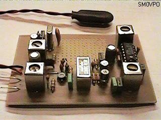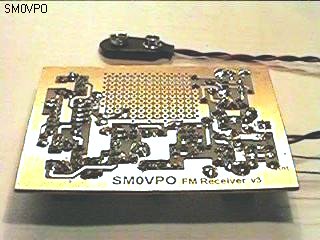

Here is a nice little receiver for narrow-band FM reception. It can also be used to receive FSK, RTTY and PACKET signals from the HF bands. Basic receiver sensitivity is in the region of 1uV PD and the receiver can be tuned to almost any frequency from 100KHz up to probably 120MHz. Ok then, here is the circuit diagram:


It is a bit big and cramped, but I think you will have no difficulties reading it. The receiver is built on a single- sided PCB, which is quite unusual for this type of circuit. I do have a PCB available, but more about that later. The RF transformers T1 & T2 and the capacitor Cy are chosen for the frequency you are interested in. As an example, using re-wound IF transformers (from Antique Electronic Supply, Tempe) the former is about 3.5mm Dia. and 10 turns (thin wire) plus Cy=33pf tuned 26MHz to 35MHz. This covers CB, 10-meters and the radio control bands.

Although the circuit looks quite complex it is really very simple. The first transistor is a harmonic oscillator so arranged that it will oscillate at any valid harmonic of the crystal. Replacing the crystal with a capcitor will result in VFO operation but the frequency stability is not so good. The oscillator and antenna tuned circuit, T2, are fed into a dual-gate FET where mixing takes place and produces the 455KHz IF. This is filtered by the CFK455 ceramic filter, amplified by the next two transistors and presented to the TBA120 (pins 13 & 14) which does all the rest. It delivers AF from the output, pin 8. Without the 10uf output capacitor you can see a DC shift corresponding to the frequency shift of the input signal. All NPN transistors can be replaced with almost any NPN transistor, such as the 2N2222 etc.
Due to the choice of IF, the wanted and image frequencies are only 910KHz away from each other. This means that with just one tuned circuit in the antenna circuit the image rejection will be poor for frequencies above about 20MHz. I thought that doesn't worry me because there are fewer stations above 20MHz to worry about. Image rejection is quite reasonable on the prototype at 14.1MHz but there was almost no image rejection at 100.455KHz. If you want a better image rejection at HF then I suggest you add another tuned circuit in the antenna circuit. Consider a converter circuit if you want to receive VHF or UHF bands above 100MHz.

There is a section of "blob-board" on the PCB that can be used to build. This board is intended to be used in a variety of applications so the complete receiver becomes a building- block that may be used to make:
I will post a few practical circuits later for some of the above applications, but my first task is an FSK to RS232 driver (Baycom compatible) so I can have a direct link to my brother G0TLA in England. This uses just two x 741 Op-Amps, one to generate -8v from the battery, the other to give +/- 8-volts signalling for feeding pin-3 of a serial COM port of the computer.

I tried to add an RF amplifer but it wasn't needed; the RF sensitivity is about 1uV PD without it. I have added the PCB foil to the DOWNLOAD section together with the component overlay. In the component overlay all tuned windings are marked "P" and link input/outputs are marked "S". The approximate coil winding ratio's are given beside T1 and T2 in the circuit diagram. T1 and T2 I wound on IF transformers from AES (part No: IL-100 at US$0.95 for a pack of five). In the prototype, T1 and T2 are wound according to the following table:
| Frequency | Coil | Primary | Tapping | Secondary | Cy |
|---|---|---|---|---|---|
| 13-19MHz | T1 | 11-turns | 1-turn | 3-turns | 33pf |
| 13-19MHz | T2 | 11-turns | none | 2 turns | 33pf |
| 19-27MHz | T1 | 11-turns | 1-turn | 3-turns | 15pf |
| 19-27MHz | T2 | 11-turns | none | 1-turn | 15pf |
| 26-35MHz | T1 | 11-turns | 1-turn | 3-turns | 8.2pf |
| 26-35MHz | T2 | 11-turns | none | 1-turn | 8.2pf |
| 33-43MHz | T1 | 7-turns | 1-turn | 2-turns | 6.8pf |
| 33-43MHz | T2 | 7-turns | none | 1-turn | 6.8pf |
| 100MHz | T1 | 4-turns | 1-turn | 2-turns | 5.6pf |
| 100MHz | T2 | 4-turns | none | 1-turn | 5.6pf |

The crystal oscillator (BC547 + T1) will oscillate at the crystal cundamental frequency or the 2nd, 3rd, 5th or 7th harmonic of the crystal. A 30MHz crystal will therefore oscillate at 10MHz, 20MHz, 30MHz, 50MHz or 70MHz. It is just to select the right Cy and T1 turns. The receive frequency will therefore be 455KHz above or below the local oscillator frequency (eg. 10MHz xtal will receive 29.545MHz or 30.455MHz with T1 tuned to 3rd harmonic). Select T2 and Cy to tune the frequency you want to receive. Crystal cut for resonance at a fundamental will function on the 5th and 7th harmonics but crystals designed for fundamental use may not oscillate at these harmonics.

Here is a photograph of one of the first basic prototypes (without any clever add-ons). The prototype looks a bit messy because I have done quite a lot of "hacking" to prove it's operation on different frequencies. I have not tried it above 100.455MHz so I do not (yet) know if this receiver will work in the 145MHz band. If you do have a go then let me know your experiences. If you also find another use for this receiver then let me have the circuit and "blob-board" layout and I will post it (with full credits) to this article.


Easy! Adjust T3 and T4 for maximum received noise then put a 10mA meter across the 100R resistor feeding the oscillator. Adjust T2 for the deepest DIP. The dip gets deeper then suddenly vanishes, wind back T2 a little until the dip suddenly appears again. Inject an RF signal of sufficient level to give a slightly noisy signal and tweek T1 and T3 for minimum noise, reducing the generator level to keep the signal weak and noisy. Now adjust T4 for maximum UNDISTORTED receive signal. The continuous FM deviation should NOT exceed about +/-2KHz with the components shown.

Have fun with this circuit. Very best regards from Harry - SM0VPO
Return to INFO page