| Back to previous page |
Gollum´s Crystal Receiver World |
Zurueck zur Vorseite |
by Berthold Bosch, DK6YY
(First published in German in 1993/94; see references at end)
Contents: 1.Voltages and Powers in Set, 2. Antenna/Earth as Signal Source, 3. Set with Parallel- Tuned Circuit, 4. Diode Properties, 5. RF Matching, 6. AF Matching, 7. Computer Simu- lations, 8. Series-Tuned Circuits .
Since my schoolboy days I have been fascinated by crystal radio reception: radio in its most basic form. However, in many cases I was not really satisfied with what I read on the subject in the literature. In the treatises I came across, the descriptions often remained rather vague, presenting little convincing foundations. Partly they were rather speculative and even presented contradicting conclusions. For this reason I found it advisable to carry out my own investigations. My intention was to obtain more quantitative results, for example as regards the best diode and the understanding of the obvious interdependence between the radio-frequency (RF), audio-frequency (AF), and DC subcircuits, what it meant for an optimum design. In the following I present results obtained over the years. Only medium-wave reception is considered.
1.Typical Values of Voltages and Powers in Set
Let us first see of what order of magnitude the RF and AF voltages and powers are which we have to deal with.
According to amplitude-modulation theory, the AF power contained in the total AM signal of power PRF is given by m2 PRF / (2+m2) where m is the modulation factor. If we assume m=0.5 we thus have 11 percent of AF power in the AM signal. Sometimes broadcasting stations use modulation factors of up to m=1 (100 percent) which then causes a correspondingly higher AF power component. At my urban location, in the West of Germany (Ruhr District), the strongest station (15 km away) produces an electric field strength of 0.18 V/m and, with my antenna and earth arrangement, an RF power of about 3 mW is available in the crystal set. Hence 330 µW of AF are contained in the RF if we assume m=0.5. A practical (linear) diode detector coupled to a tuned circuit delivers 70 to 80 percent of this to the AF load. This means that ideally I can expect about 240 µW of AF being available from my local station, sufficient for moderate operation of a loudspeaker.In the crystal set that I am going to investigate (Fig. 2 below) I measured the following RF voltages across the tuned circuit when RF and AF matching existed (Secs. 2, 5 & 6):
a) Tuned to the local station (WDR 2, 720 kHz, 200 kW, 15 km away):8.9 V
b) From of my "district station" (DLF, 549 kHz, 100 kW, 35 km, field strength 40 mV/m, 0.2 mW of RF power):2.3 V.
c) At night - with a wave trap for the local station - more than a dozen stations appear from all over Europe with 1 to 5 mV/m, producing 130 mV across the circuit as a mean value (0.5 µW of RF). Such low voltages will move the working point over only a rather limited part of the diode characteristic where the relative curvature is low. Consequently, the detector efficiency now drops to below one percent.
d) Good headphones produce an audible signal down to 10 pW of applied AF power. Employing a signal generator and using a sensitive diode (see below) I found that an RF power of about 10 nW is required to generate this 10 pW of lower-limit AF. The detector efficiency has at this very low RF level thus fallen to a mere one per mille. Obtaining an RF power of 10 nW in my set requires a field strength of about 0.3 mV/m. According to estimates based on groundwave propagation theory, a 1000 kW transmitter operating near 1500 kHz should generated 0.3 mV/m at a distance of 190 to 200 km; the electric field strength is roughly proportional to Radicle (PTX)/(f2d2), where PTX = transmitter power, f = frequency, and d = distance. The particular example is chosen because at 1440 kHz I can during the day just hear the signal of RTL Luxembourg, being 195 km away and reported to radiate 1200 kW. The voltage measured across the tuned circuit was 40 mV in this case. To be able to receive RTL I carefully have to suppress the local as well as the district station.
e) When I connect an AF amplifier to the crystal set, a number of stations located about 150 to 250 km away can additionally be heard via groundwave propagation in the daytime. The diode thus provides (some) detector action at RF levels even lower than 10 nW. But the AF power generated is then too small to produce an audible signal in the phones directly.
The above numbers show the considerable variations in the RF voltage generated across the tuned circuit. Hence it is not surprising that a crystal diode found to be best suited for DX reception is not necessarily the optimum choice for achieving best loudspeaker operation from the local station. But before I present results on diode behaviour I am going to describe the circuit I employed. Let us start with antenna and earth as an integral part of the total circuit.
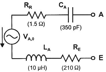
2. Antenna and Earth as Signal Source
(Fig. 1: Equivalent circuit of antenna/earth combination.)
I use an inverted L-type antenna of 43 m length, about 10 m above ground. The earth connection is provided by three metal rods of 2 m length each, driven into marly, i.e. a not particularly well conducting, soil. The antenna/earth combination can be represented by the equivalent circuit shown in Fig. 1, giving measured values for the various elements. The antenna capacitance is denoted by CA, the inductance by LA, RE is the earth loss resistance, RR the radiation resistance, and VA,O the antenna source voltage. The two last elements increase in value with the antenna's height and length. For the source voltage I measured a value of 1.6 V, using a selective RF voltmeter. The knowledge of this quantity, which is produced by the strong local station, permits to easily determine the earth resistance. For it 210 ohms were obtained, a relatively high value. Reducing it by installing a better ground system would pay high dividend.
Maximum power is transferred to the load, i.e. from the antenna to the crystal set connected to A-E, when we arrange for impedance matching and for resonance in the resultant antenna/earth series circuit. The set will presents, in general, an inductance which is too small for achieving resonance in the antenna circuit. Therefore, an additional coil must be inserted (Fig. 2). The resistance of about 400 ohms in the series-tuned circuit (200 ohms source resistance plus 200 ohms resistance of set when matched) yields a Q-factor of only 4. But this is still helpful regarding sensitivity, but also selectivity (sharpness of tuning), since the delivered current (voltage) is increased by this factor of 4, meaning 16 times in power.3. Crystal Set with Parallel-Tuned Circuit
As a sort of "standard set" I used and investigated the popular arrangement shown in Fig. 2 which employs two tuned circuits. The inductance LC couples the antenna to the coil of the tuned circuit, the degree of the variable coupling chosen so that matching is achieved. The fixed L1 has a somewhat larger value than required for tuning the antenna/earth circuit of Fig. 1. The variable capacitor C1 is then used for tuning to resonance. The numbers for L1 and C1 apply to my particular case. C3 serves as AF storage capacitor for obtaining a maximum of AF amplitude at the phones, and it additionally provides a short for the RF. In practice, however, it often can be omitted without audible drop in AF. - To be able to properly match the diode detector to the parallel-tuned circuit, the detector branch is hooked up either to the top of coil L2 (wound with Litz wire onto a suitable ferrite rod) or to one of 11 taps provided on it. In this way the diode can be connected, via a switch, to 12 resistance values along the tuned circuit. Such a fine adjustment was required for the investigations reported in Sec. 5. The unloaded tuned circuit has a resonance resistance of 105 k ohms (at 1000 kHz), which drops to 52 k ohms when matched to the antenna/earth. (These are not particularly high resistance values because of the many leads from the taps to the switch.) According to the switch position chosen the diode can so be connected to 12 resistance values that vary between 52 k ohms and 100 ohms. When the diode is set to the tap that provides matching the total resonance resistance then drops to 26 k ohms. - On the right in Fig. 2 the equivalent circuit of the headphones is given which we require later on.
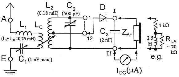
(Fig 2: Wiring diagram of crystal set with parallel-tuned circuit and tuned
antenna/earth.)
We have now the task to match (1) on the RF side the diode branch, via the tuned circuit and the antenna coupling, to the antenna source, and (2), regarding the AF, the phones or the loudspeaker to the diode. Both procedures are strongly interrelated. But first we must find out more about the diode and its dynamic resistance.
4. Crystal-Diode Properties
All semiconductor diodes principally show a dependence of current I on
applied voltage V (static characteristic) like I=IR,0*exp (V/nVT)
- IR,0, where IR,O denotes the reverse saturation current at high
negative voltages, VT the temperature voltage of 26 mV at room
temperature, and n an ideality factor between 1 and 2.
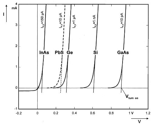
(Fig. 3: Theoretical current-voltage characteristics of various p-n diodes; equal diode areas assumed.)
Reverse breakdown is neglected. The relationship applies to both to p-n diodes and to Schottky diodes. However, the composition and physical meaning of IR,O differs completely for these two diode types (diffusion current resp. field current). Important is the fact that the exponential rise of the diode current occurs the faster, i.e. the turn-on voltage (as a kind of threshold) becomes the lower, the higher the saturation current IR,O is. Calculated characteristics for p-n diodes made from germanium, silicon, two modern compound semiconductors and from galena (PbS) are given in Fig. 3, assuming equal diode areas. The associated reverse currents are stated. The difference in diode behaviour is caused by differing electronic material properties (band gap). Real curves, in particular of the natural crystals, are flatter because of parasitic elements, mainly of diode series resistance. Regarding low turn-on voltage a galena p-n crystal diode is theoretically even slightly better than one made from germanium.
For Schottky diodes principal curves like those in Fig. 3, relating to a particular
crystal material, cannot be given. In their case the characteristics strongly
depend on the kind of the metal electrode and on the processing parameters.
But measured curves for Schottky as well as for p-n diodes are given
in Fig. 4, including fairly good examples of galena (PbS) and iron pyrite (FeS)
detectors; see also the Table below for identifying the diode types. Again one
notices the relatively low turn-on voltage of the two natural crystals which
equal or even are below that of the germanium diodes 1N34 and OA5, thus being
well suited for low-level detection.
(Fig. 4: Measured current-voltage characteristics of various semiconductor diodes
(reverse currents indicated))
Very interesting is the performance of modern low-barrier Schottky diodes made from silicon, like the NEC 1SS16 (almost identical: 1SS99, BAT32, BAT63), which show turn-ons at 0.15 to 0.18 V. And, indeed, they show superb performance at low levels. One should expect that the InAs Schottky diode (which was specially made for my experiments) and the TU 300, a backward diode made by Siemens, would according to the curves shown be even more sensitive detectors. But this is not the case.
As mentioned, a low turn-on voltage is inevitably associated with a high reverse current. This current reaches values of a few hundred µA for the InAs diode, as also for the TU300 and the Schottky diode BAT33. If the reverse current, i.e. an unwanted back current, reaches such high values we have strong counteracting effects, and ultimately the detector action disappears completely. Anticipating the results of computer simulations described in Sec. 7 one can state that diodes like the 1SS16 show the optimum relation between low turn-on and still acceptable reverse current, thus making them the best choice of presently available diodes as regards detector sensitivity.
To show and compare the capability of various diodes the Table summarizes values of measured AF voltages and of rectified currents, for 1 and 100 µW of available RF power. A power of 1 µW is in my set typical for DX stations at night, and 100 µW for stations 30 to 50 km away. As is seen the 1SS16 leads the field. - For 3 mW of RF (my local station) I obtained with a 1SS16 a DC current of 715 µA, which increased to 1.85 mA in the short-circuit case (AF/DC load = 0), and to 2.95 mA when under these conditions the set was retuned.
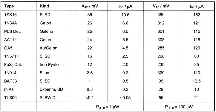
(Table: Measured values of AF voltage (across phones of 4 k at DC) and of rectified DC current for various diodes and two levels of RF power)
Sometimes a DC bias from a battery is applied for shifting the operating point of the diode closer to the turn-on voltage and so improving the detection efficiency. By this method the AF voltage obtained can be increased, for example when using the 1N5711 and the 1N914 at low RF levels. The 1SS16 group of diodes, however, hardly gains from a DC bias. Only at RF powers below about 200 nW I was able to measure a certain rise in AF voltage. At the lowest detectable RF level of 50 nW (Sec. 1), the AF voltage increased by 20 percent (i.e. power by 45 percent) when the optimum bias was applied. But this effect was measurable only, being still too small to be noticed by the ear.
Note added in Jan. 2002: Backward diodes (BWD), like the TU300, are good detectors at extremely low RF signal levels, below about 1 nW with associated voltages of only a few mV. This is due to the relatively sharp bend in the BWD characteristic at zero volts. The generated AF signal is, however, too small for operating phones directly and calls for an AF amplifier. Then stations can be copied which are not heard when in such a set-up with AF amplifier a "normal" sensitive diode, like the 1SS16, is used instead of the BWD.
5. RF Diode Resistances and RF Matching
For achieving best performance it is required to RF match the diode to the tuned circuit. The dynamic resistance of the diode depends on the amplitude of the RF voltage applied to it, and on the kind of AF load impedance.
In AM tube radios the detector diode operates at a high level (linear detection) and has a load consisting of a large (ohmic) resistor shunted by a small capacitor. Calculations show that in this case the RF diode resistance, as presented to the tuned circuit, is roughly half of the ohmic load resistance. In a crystal set the calculation is somewhat more complicated since there the RF voltage on the diode is generally lower and the diode load is more complex (see equivalent circuit of phones in Fig. 2). Hence I preferred to measure the RF diode resistance RD. The measurements were carried out under actual working conditions using a signal generator. Figs. 5(a) and (b) show the results obtained for high-impedance phones with 4 k ohms DC resistance and for low-impedance ones with 120 ohms, respectively. The RF frequency used in these measurements was 1000 kHz, the modulation frequency 1 kHz with a modulation factor of 0.4 (given by the signal generator). Figs. 5 give the measured diode resistances, as a function of the RF power applied, for an 1SS16 (also some in parallel), a silicon p-n diode 1N914, and for natural galena as well as carborundum (silicon carbide; SiC) crystals. The diode circuit was in turn connected to the various taps on the coil L2 .When the RF voltage measured across the tuned circuit dropped by a factor of radicle (2)=1.41 compared to its value without diode, matching was achieved. Then the RF diode resistance equalled the RF resistance of the tuned circuit at the tap point. To avoid an error one must readjust the coupling to the antenna when the diode is connected to the first found (V/1.4) tap point and then repeat the search for the now somewhat altered (V/1.4) tap. A second iteration further improves the result, but not much.
As in principle to be expected from the characteristics, the diode resistances
vary rather widely, from some 100 ohms to some 10 k ohms, with lower values
obtained when the DC resistance of the phones is low. The galena detector shows
values only moderately higher than those of a single 1SS16. The silicon diode
1N914 presents high values due to its high turn-on, which even more applies
to carborundum.
(Fig. 5:Measured RF diode resistances versus available
RF power: (a) for high-impedance phones (4 k ohms at DC),
The data obtained then indicate that the optimum tap position on coil L2 (for matching) depends on the diode type, the strength of the received station, and on the DC resistance of the phones. The larger the value of the diode resistance is, the higher must the tap position be up the coil. Sometimes it was suggested in the literature to have a fixed tap at a point of about 1/4 to 1/3 of the windings counting from the earth point. In the present case the tuned circuit has a resistance of approximately 6 k at the 1/3 tap point. As Fig. 5a shows, this indeed is a rather good choice for a galena detector when high-impedance phones are used and weak stations received. Impedance matching requires that the reactances of source and load cancel out. But in our case the resistance of the tuned circuit has no reactive part at resonance, and the reactance of the diode, caused mainly by the diode junction capacitance of at most a few pF, can be neglected.
Connected to a particular tap, the diode resistance is (auto-)transformed up and appears in parallel to the resonance resistance of the tuned circuit. This means that not all of the available RF power reaches the diode since a reasonable fraction of it is dissipated in the resistance of the tuned circuit. In order to really transfer the maximum of power from the antenna to the diode branch, the diode (of generally low resistance compared to that of the tuned circuit) should be connected untapped to the top of the coil L2. This, however, strongly reduces the selectivity of the set and requires a readjustment of the coupling of the tuned circuit to the antenna. With high incident high RF power (and/or low impedance of the phones) the tuned circuit can, under these conditions, become loaded to such an extend that variations of the capacitor C2 have no tuning effect any longer, which means that C2 is obsolete and can be omitted. The diode circuit is then aperiodically coupled to the (tuned) antenna circuit, while the coil L2 merely acts as the secondary winding of the transformer which matches the diode to the antenna.
6. AF Matching
If a crystal ear phone is used or the diode detector is followed by an amplifier (generally of high input impedance) one has to design for maximum voltage at the detector output. Here, we rather have to deliver a maximum of power to the phones. Hence the impedance of the phones (or the speaker) as the AF load should have such a value that a maximum of AF power is transferred to it. The AF source resistance RG is at low RF levels (square-law detection) approximately given by the reciprocal of the slope of the diode characteristic at the operating point. At higher RF levels (linear peak detection) it is determined by the current spikes flowing through the diode. In so far, RG nearly equals the diode resistances as shown in Figs. 5. The tuned circuit presents an AF short.
I determined the equivalent circuit of a pair of high-impedance Telefunken
phones (4 k ohms at DC) at 1 kHz by using a measuring bridge and obtained the
quantities given in Fig. 2. REA is caused by the electro-acoustical transducing
process. The AF source has to provide the real power for REA as well
as, necessarily, for the DC coil resistance, and foremost the reactive power
for the phone coils (2.5 H) that are to move the membranes. In order to obtain
the maximum of power transfer the magnitude (amount) of the overall phones´
impedance ZAF ( 16 k ohms for my phones) must match the AF source. Again
I preferred to experimentally find the optimum AF load: I connected in turn
14 phones and speakers of different impedance to the set, partly connecting
two of them in series or parallel, which in total provided 20 load impedance
values between 80 ohms and 75 k ohms in magnitude. From the AF voltage measured
across these load impedances I determined the AF power. The coupling to the
RF signal generator was readjusted to retain RF matching each time the AF load
was changed. Fig. 6 shows the obtained results when using a) a diode 1SS16 at
low RF power (1 µW) and b) with a 1N914 at higher power (1 mW). The optimum
AF load impedance turned out to be, resp., 1.2 and 3 k ohms. In order to simplify
matters the diode was in this experiment fixed to the 1/3 tap at the tuned circuit.
This meant a compromise as regards match-ing and generally did not produce quite
the maximum of achievable AF power. The dashed curves of higher AF power in
Fig. 6 were obtained when the diode was connected to the top of the tuning coil
(as discussed above). 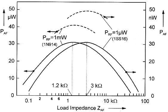
(Fig. 6: measured AF power versus AF load impedance.)
In order to present my measurement results in a more general form, Fig. 7 shows the AF power obtained as a function of the AF impedance now divided by the respective occurring source (= diode) resistance. The curves indicate that the maximum is reached when ZAF has a value of 50 to 70 percent of the diode resistance. The simplifications introduced above, like choosing the fixed 1/3 tap, are probably the reason for not reaching a higher percentage. But we can say to be roughly correct with our predictions. - Sometimes it is suggested to match just available phones (speaker) to the diode by using a suitable transformer. I found this only helpful if the mismatch was extremely high. In the other cases the winding and iron losses of the transformer, as well as the inductive shunt, tend to dissipate more AF power than is gained by providing the right transformation ratio. One also has to consider that the human ear cannot register small changes in acoustical power. Alterations like those shown above the dashed line in Fig. 7 will hardly be noticed by the ear. Thus, it seems that the exact value of the AF load impedance is not of paramount importance as regards noticeable output power. But the general principle holds that a number of small improvements in matching, each of which will not produce any audible effect for itself, might in sum indeed be noticed by the ear.
So it turns out as an interesting and important feature that a high-impedance AF load, which is associated with a high DC resistance, will produce a high diode resistance (= AF source resistance), and vice versa. This means that the circuit has a self-optimizing tendency towards the matched condition. Regarding RF selectivity of the set, as another important quantity, a high AF impedance - leading to a high diode resistance - is of advantage. But the influence of the AF impedance in this respect is not particularly pronounced. I measured an increase in -3db RF bandwidth by a factor of 2.5 when the AF load was decreased from 100 k ohms. At 720 kHz (local station) this bandwidth was 20 kHz in my set, which yields a total loaded Q factor of 36 - leaving room for improvement (see Secs. 2 & 3).
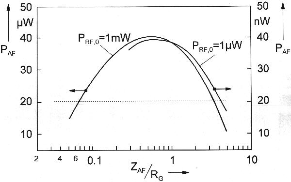
(Fig. 7: Measured AF power versus AF load impedance normalized to AF source resistance.)
7. Computer Simulation of Crystal-Set Behaviour
As a summarising investigation I simulated the overall performance of the circuit shown in Fig. 2, using the analysis program SPICE. An RF frequency of 1 MHz, an AF of 1 kHz, and a modulation factor of m=0.4 were assumed. The tap on the coil L2 was held fixed at 1/3 of the windings from earth. The I(V) equation given in Sec. 4 served to describe the diode behaviour.
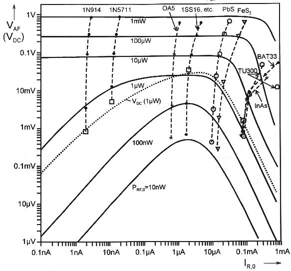
The simulation results are presented in Fig. 8, which shows the AF voltage VAF AF obtained across phones of 16 k ohms AF impedance (4 k ohms DC) as a function of the diode reverse saturation current IR,O. Parameter is the available RF power at the tuned circuit, ranging from 10 nW (lowest sensible level; see Sec. 1) to 1 mW (about local-station level). Measured values pertaining to various diodes are entered for comparison. These measurement values lie in part slightly below, partly somewhat above the simulated curves, but agree in general. In practical diodes, particularly Schottky diodes, the effective reverse current increases noticeably with reverse voltage (i.e. with increased RF power). This had to be considered when inserting the measured values in Fig. 8, and accounts for the slight bending of the vertical lines to the right. The dotted curve in Fig. 8 shows the simulated DC voltage across the phones for 1 µW of RF power.
The simulated curves for VAF drop at the right side for diodes with high IR,O because of the adverse effect of reverse current as mentioned in Sec. 4. The decrease at the left of Fig. 8 for low RF powers results from the high turn-on voltage shown by diodes having a low IR,O. In these cases the associated smaller RF voltages increasingly fail to reach the turn-on of the diodes. The curves make clear how important it is to choose a diode which has the right value of reverse current. A definite maximum in sensitivity, especially pronounced at low RF powers, is found for diodes having a reverse saturation current of a few µA. Particularly the 1SS16 diode class is in this range, but also the OA5 and 1N34 perform not too badly, and good specimen of galena (PbS) crystals behave still satisfactorily. Hence this result is quite in agreement with what we already have found in Sec. 4. - When the AF voltages in Fig. 8 are used for calculating the AF power, the AF/RF detection efficiency can be worked out. It is found that the efficiency drops drastically for low RF levels, with one per mille being reached at 10 nW of RF. This agrees with the observations described in Sec. 1.
In the simulation the reverse breakdown voltage, at which in practical diodes the current starts to rise rapidly, was not included. For 1 mW, the highest RF power considered, the diode resistances have dropped to around 3 k ohms (Fig. 5a), calling for a low tap position on the coil. There the RF voltage is relatively low. My local station, with 3 mW of RF, produces 2.4 V (i.e. a peak-to-peak value of 6.7 V) at the required tap point, so that the negative peak only just reaches the breakdown voltage of -6 V for a 1SS16. In consequence, reverse breakdown seems not to be a particular limiting factor, even if the voltage across the tuned circuit might be somewhat higher in case there is a better Q factor. Assuming a constant available RF power, the RF voltage is proportional to the square root of the Q (resonance resistance). The low-barrier silicon Schottky diodes, which show a reverse breakdown in the range of -5 to -8 V, are thus well suited for use from the lowest to the highest levels of RF power generally occurring in crystal sets.
8. Some Remarks on Series-Tuned Circuits
Historically the first crystal sets, in the pre-broadcasting days, were of
the kind shown in Fig. 9a. There the values of L1 and C2 pertain
to my particular antenna/earth situation. For maximum power transfer in the
circuit of Fig. 9a the combination of crystal plus load in parallel should match
the impedance of the antenna source. In the latter the earth resistance represents
the main resistive part which in the then primarily commercial stations had
values of only 10 to 50 ohms. On the other hand, the crystal-diode resistances
were around a few k ohms so that a considerable mismatch existed. For this reason
one soon changed to the arrangement of Fig. 9b with diode and load now in series,
and with the possibility to match the diode branch to the antenna by choosing
the right tap on the coil L1. To increase the selectivity of the set
a second tuned circuit was eventually introduced, as e.g. shown by Fig. 2.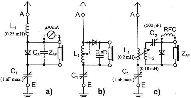
(Fig 9: Series-tuned circuits: a) Diode directly in tuned antenna circuit, b) Diode across tuning inductance (preferably tapped), c) Diode in separate series-tuned circuit, coupled to the series-tuned antenna/earth circuit.)
Using modern low turn-on diodes (1SS16 etc., Sec. 4) and having in general a higher earth resistance than in commercial stations, the circuit of Fig. 9a is however quite effective. Possibly paralleling of diodes is of advantage, depending on the actual source and load resistances. With two 1SS16 and employing a moving-coil speaker via a suitable transformer as the load I obtained an AF power of 180 µW from my local station. With ten 1SS16 and two moving coils of 16- ohms speakers in series as load, the obtained AF power of 210 µW approached the maximum possible after Sec. 1. Ideally the diode resistance should, in my case, about equal the 210 ohms of the antenna source (Fig. 1). Reverse diode current is not harmful, nor a possibly low reverse breakdown voltage. We have here a “current-controlled” case where voltages across the diode remain low with associated high currents, a few tens of a mV and some mA when I used the ten diodes. In contrast, voltage control is - more or less - experienced when parallel-tuned circuits are employed where high(er) voltages and low(er) currents exist. A set according to Fig. 9a, then, is a most simple hook-up for effectively receiving the nearest station. Substantially higher selectivity, approaching that of the set of Fig. 2, is offered by the arrangement with two series-tuned circuits shown in Fig. 9c. Since there any resistance (loss) in the circuit made up by L2 and C2 should be kept low for achieving a high Q factor, the diode(s) - preferably paralleled again - and the phones/speaker should be of low impedance. The RF choke might help to improve performance. The diodes found in the left of Fig. 4, particularly the backward diode TU300 (which is of little use on parallel-tuned circuits), operate excellently in the arrangement of Fig. 9c. Modern 8/16- ohms headphones or, for stronger stations, directly the moving coil of a speaker are effective AF loads. - Backward diodes, being scarce these days, are tunnel diodes which have the typical current hump reduced to a flat region at about 200 µA height. The I(V) curve of the TU300 shown in Fig. 4 has in reality reversed polarity. For reasons of comparison with the other diodes the polarity was changed in the graph. Other BWD types are: AEY17 /29, 1N3539 /3543, TU1B.
In conclusion, the investigations sketched here have certainly enlarged my knowledge on crystal-set design, with the identification of the “best diode” and noticing the tendency of self-optimization which makes the set a sort of good-natured device. Other rewarding topics could not be covered, as there are, for example, more complex circuits for increased selectivity and for DX. Also short-wave crystal sets are fascinating since they provide DX from all over the world with simple designs.
Based on:
B. Bosch and M. Bussmann: Zur Empfindlichkeit von Kristallgleichrichtern und Halbleiter- dioden beim Detektorempfang.Funkgeschichte Nr. 93 (1993), pp. 275 - 285.
B. Bosch: Anpassungs- und Schaltungsfragen beim Detektorempfang.Funkgeschichte Nr.98 (1994), pp. 211 - 225.