|
How to Reduce Diode Detector Insertion Power
By Ben H. Tongue
Quick Summary: Diode detector insertion power loss can be reduced below the value achieved under impedance matched conditions. The requirements are: (1) Output load resistance equals twice the RF source resistance. (2) The Saturation Current and Ideality Factor of the diode are such that the very-low-signal output resistance of the detector equals the output load. It is usually assumed that power loss in a two port device (here, a
crystal set) is minimized when its input and output ports are impedance
matched. This article will show that this is not true in the case
of a diode detector operating at a signal power level well below that of
its region of essentially linear operation. In the linear region
audio output power is proportional to RF input power. That is, for
every dB of change in input power there will be one dB change of output
power. In the lower power region, called the 'square law' region,
a change of one dB in input power results in a two dB change in output
power.
Definition of terms: Rd: Resistance of a diode at its axis crossing. Rd=0.0257*n/Is at 25 degrees Celsius
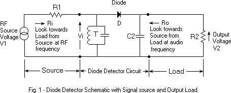
It has been asserted in previous Articles that the RF input and audio output resistances, Ri and Ro, of a diode detector approach the same value and equal 0.0257*n/Is = Rd ohms at room temperature when the input signal strength is low enough. See Article #0, part 3, Article #4, part 2 and Article 16 for information on Is and n, and ways of measuring them. Fig. 1 represents a conventional diode detector. The tank circuit T is shown with no internal loss. A real world tank will have loss that can be represented by a shunt resistor connected across it. For convenience of analysis it is assumed that this loss resistance is absorbed into the source V1, R1 (For a more complete explanation, see Article #1, first paragraph after the third schematic.). Impedance transform the source (antenna) and load (headset) resistances to equal values (R1 = R2) and select a diode that has an Rd equal to them. This will result in a reasonable impedance match at both the input and output if the signal power level places operation below +10 dB of the linear-to-square law crossover point. Little input power directed towards the detector will be reflected back to the source and most all of the output power from the detector will be absorbed in the load, R2. If the diode detector were a linear device with linear input and output resistances, this impedance-matched condition would result in the least detector power loss (greatest sensitivity) obtainable. It would seem clear that the crystal set detector cannot be made more sensitive. Actually, not so! Very weak signal sensitivity can be improved, theoretically, by about 2 dB while using the same power source (V1 and R1). This gives a hard-to-hear increase in volume, but every little bit helps. In the impedance matched condition discussed so far, R1=Ri=Rd and R2=
Ro. Simple math shows that the detector input voltage Vi will equal
one
half the internal source voltage V1. If we create an impedance
mismatch between the source resistance R1 and the detector input resistance
Ri by replacing the diode D with a different one having one-half the saturation
current, Vi will increase. The reason is that the detector input
resistance Ri is now twice R1 and the voltage divider made up of R1 and
Ri will reduce V1 by only one third at the input of the diode..
A higher input voltage to the diode should result in a higher output power
to the load R2. Since the new diode will have double the output resistance
than the old one, all of the benefit from the greater value of Vi could
be lost by the greater voltage division between the (now two times higher)
detector output resistance and the load R2. All is not lost, however,
since the detector is operating in the square law (weak signal) region.
Even though the two voltage division actions tend to cancel (for small
changes), the detector output will be higher because of square law operation.
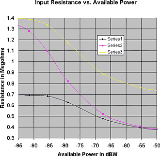
Theoretical calculation and Spice simulation show that that in a crystal set having equal values for R1 and R2, the diode parameters that give to lowest insertion power loss at low signal power levels fit the equation: R1=R2=2*(0.0257*n/Is)=Rd at room temperature. Now let us look at the effect on Ri and insertion power loss if Ri does not match R1. Look at Fig. 2.
What does all this mean?
|