A New Diode Detector Equivalent Circuit with Equations
for Calculating a Detector's Linear-to-Square Law Transition
Point and its Insertion Power Loss.
by Ben H. Tongue
| Quick Summary: The purpose
of this article is to describe and compare a new diode detector equivalent
circuit to a real world detector. This equivalent circuit uses an
ideal diode. The comparison is made using SPICE simulations of the
two circuits. The concept of the 'Linear-to-square-law crossover'
point in the relation between output and input power is introduced (not
to be confused with the exponential relationship of current to voltage
in a diode). |
|
Part 1: General Description of a Diode Detector.
The new diode detector equivalent circuit is based on the idea that
a detector diode imbedded in a proper circuit can be thought of as a device
that converts RF power into DC power. Some power is lost in the process
and that is called detector insertion power loss (DIPL). This
approach completely avoids such concepts as duty cycle, pulse current,
bypass capacitor charging and non-linear instantaneous voltage/current
relationships. It is also consistent with the material given in Article
#1. The peak-detector, capacitor-charging-current line of thought
is good when signal levels are high enough to assure that true peak detection
occurs. It is not very useful when signal levels are low. However,
when all is said and done, the more different valid ways one can use in
thinking about how a circuit works, the better becomes one's understanding
of that circuit.
This analysis applies to an AM detector fed by a CW RF sine wave voltage
of frequency fo: It has a peak (not RMS) value equal to V1 and an
internal source resistance of R1. The "maximum available RF input
power" is called P1 (see section 2 in Article #0 for info on "maximum available
power"). The DC output power delivered to the load resistor R2 is
called P2. The DIPL (in dB) is equal to ten times the log of the
ratio between the two powers P2 and P1.
This approach can also be used to model how a diode detector behaves
with an AM modulated input signal by performing a SPICE simulation three
times. Once with the RF signal equal to the value of the desired
modulated wave's envelope minimum value, once with the signal equal to
the carrier value and once with the signal equal to the crest value.
The three DC output voltages give the minimum, carrier equivalent and peak
value of the demodulated output audio wave.
***** Please do not skip this next paragraph! *****
To understand the new diode detector equivalent circuit, one must abandon
the usual way of thinking the about the diode in a detector. Instead,
one must think about the "diode detector circuit". This circuit
includes a tank circuit T, the output capacitor C, as well as the diode.
The shunt input reactance of the circuit is assumed to be zero at all frequencies
except fo, the frequency to which the tank is tuned. The input
resistance at fo will be discussed later. The output reactance of
the circuit is assumed to be zero at all RF frequencies. The output
DC resistance will be discussed later. A real world diode is a two
terminal device. The "real world diode detector circuit" will be modelled
as a "two port, four terminal device" having a pair of terminals
for the input and another for the output. One of the input terminals is
the "hot" input terminal; the other is "low". One output terminal
is the "hot" one, the other is "low". The two "low" terminals are
connected together and usually to ground. Please note, that in the
topology of the two schematics shown below, the "Diode Detector Circuit"
and the "Diode Detector Equivalent Circuit" both include the tank
T and the bypass capacitor C2 as an integral part of the detector.
Also, look at the circuits in this way: The tank circuit, looking
towards the output, sees the diode as a one-end-grounded shunt load
since the output bypass cap is a short at RF. The output load resistor,
looking back towards the input, sees the diode as a one-end-grounded
shunt DC resistive source since the input side of the diode is shorted
to ground by the tank.
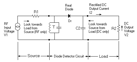
See Fig 1. The detector tank circuit T is modelled as lossless and resonant
to the input frequency fo. Losses in a real world tank can be accounted
for by using Thevenin's Theorem to calculate the appropriate changes in
V1 and R1. This leaves the circuit topology unchanged. See
Article #1 for more on this subject. The value of the tuning capacitor
in T is sufficiently large so that essentially no harmonics of fo can appear
across T. This assures that the "pendulum-like resonator effect"
of a high Q circuit will be available to supply the narrow, high-current
pulses the diode requires every cycle when strong signals are handled.
Another advantage is that tank-voltage-waveform peak clipping from diode
conduction is essentially prevented when the current pulses are drawn.
All this assures that the input impedance to the detector will be linear
and the input current to and Voltage across the tank T will always be sinusoidal,
no matter how weak or strong the input signal. See Article #8 for
an illustration of typical waveforms. A reactance value for the tank
capacitor equal to less than one hundredth of the value of R1 will be sufficient.
The DC resistance of the tank inductor should be small enough so that no
appreciable DC voltage will appear across it. A value less than one
hundredth of the value of R2 will be sufficiently small. This assures
that all of the output DC power goes into R2. The bypass capacitor
C2 has a very low reactance compared to the load resistor R2 at the frequency
fo. Since C2 acts as a short circuit across R2 at the frequency fo, all
of the RF voltage applied across T will appear across the Diode. The time
constant, R2*C2 should be long compared to the time for one cycle of fo.
The load resistor R2 absorbs the output power P2 = (V2^2)/R2.
Detector Power Loss is DIPL = 10*log (P2/P1) = 10*log (((V2/V1)^2)*((8*R1)/R2))
dB. Minimum detector power loss occurs when the RF signal source
"V1, R1" is impedance matched to the detector input resistance and the
DC load resistance R2 is matched to the detector output resistance. |
Part 2; Discussion of the new Diode Detector
Equivalent Circuit.
Actual Diode Detector to be Simulated in Spice.
|
Fig 1.
| To gain an understanding of the Diode Detector Equivalent Circuit,
first consider the following line of thought: See Fig. 1. Let
the input RF voltage V1 approach zero. V1, at a frequency fo, looking
toward the load resistance R2, will see an RF resistance (at fo) equal
to the resistance of the diode at zero bias. At the zero signal condition
this resistance is not affected if any changes were made to R2. The
value of this resistance is the slope of the diode V/I curve at the origin.
From the Schottky diode equation, the numerical value of this resistance
is: (0.0257*n)/Is Ohms at a temperature of 25 degrees C. Let's call
this Ro. Is and n are parameters in the Schottky diode equation.
(For a discussion of Is, n, etc., see the text after the schematics in
Part #1 of Article #1). From the load resistance R2, looking back
toward the input, one sees the same resistance value Ro (at DC this time),
and it is independent of any changes at the source. Now look at Fig.
2. Here, the real world diode has been changed to a theoretical ideal
diode and two attenuators of characteristic resistance Ro have been are
added. If V1 becomes zero, the attenuators A1 and A2 must be set
to infinite attenuation to enable the model to duplicate the behaviour
of the circuit in Fig.1. When an input signal is applied, the values
of A1 and A2 must become finite. The DIPL is equal to the sum of the loss
of each attenuator plus the impedance mismatch loss between the ideal diode
Di and each attenuator. SPICE simulation shows that this diode detector
equivalent circuit can do a pretty good job modelling the operation of
a real world diode detector. To verify this statement, perform a
SPICE simulation of Fig.1 and of Fig.2 with V1, R1 and R2 the same in each
case. Adjust the attenuation value of A1 and A2 = X dB to a value
that causes the output, V2, in Fig.2 to be the same as in Fig.1. This adjusts
the DIPL to be the same in each circuit. The input impedance match
of the two simulations differ from each other by less than 14% over an
input power range of 36 dB centered at the Linear-Square-Law Transition
(LST) point. The equivalent circuit seems to work for signals
from well below the LST point up to levels just before "Diode Reverse
Breakdown Current" comes into the picture. |
Diode Detector Equivalent Circuit to be Simulated
in SPICE.
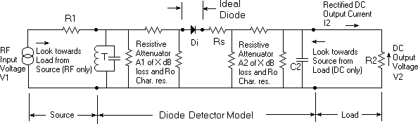 |
Fig. 2
Some definitions and conditions that apply to Fig. 2 follow:
-
Di is an ideal diode. It has zero forward resistance and infinite
reverse resistance. That is, it can pass any current in the forward
direction with no voltage drop, and it will conduct no current in the reverse
direction, no matter how much voltage is applied. Rs represents the
series parasitic resistance of the real world diode (Dr) being modelled.
It is shown for completeness, but has negligible effect on the results
at the values encountered in crystal set operation (5 to 60 Ohms) and will
be ignored.
-
A1 and A2 are "constant resistance" attenuators of equal attenuation, X
dB. Their loss is dependent on the strength of the received signal
power. The attenuators each have a characteristic resistance Ro.
Is is the saturation current of the real world diode Dr in Fig.1. and n
is its Ideality Coefficient. Note: When a "constant resistance"
attenuator is driven by and loaded by a resistance value called its "characteristic
resistance", its own input resistance and output resistance remain constant
no matter what attenuation it is set to.
-
The input and output resistances of the detector are equal to the characteristic
resistance of the attenuators. R1 = R2 = Ro.
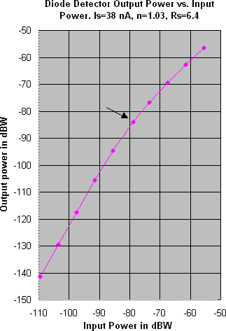
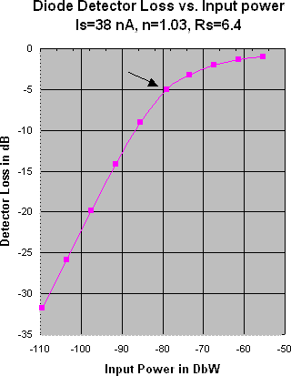
A SPICE simulation of the circuit shown in Fig. 1 results with the graphs
shown in Figs. 3 and 4. Another SPICE simulation of the circuit shown
in Fig.2 results in data shown in Chart 5, but with attenuators A1 and
A2 adjusted at each row to give the same DIPL values as were obtained with
the simulation of the schematic in Fig.1. The simulations of Fig.
1 use a Schottky diode with Is =38 nA, n=1.03, Rs = 6.4 ohms,
BV (Reverse breakdown voltage) = 15 volts, IBV (Current at BV) =
25 uA. In both circuits R1 = R2 = Ro = (0.0257*n)/Is = 700k ohms.
The value of 700k Ohms used here is very high for a crystal set designed
for use with an external antenna.. The reason is that it is very
difficult to develop a source resistance of 700k ohms without incurring
a high tuned circuit loss. The 700k value can be obtained in a high
performance single tuned loop crystal set. The simulation for Table
1 can be performed for other values of R1 = R2 = Ro. For lower values
of R1 = R2 = Ro, practical for use in crystal sets intended for use with
an external antenna, the input power required at the LST point will
be higher than that shown here, although the DIPL will be the same. |
|
|
|
Fig. 3
|
Fig. 4
|
Some data from SPICE simulations of the circuit in figure 2, for three
of the data points used in Figures 3 and 4 are shown below.
Division of DIPL between (A1 + A2) and Diode
Interface Mismatch Power Loss
in the Detector Equivalent Circuit of Fig. 2
RF Input
Voltage
V1, in mV.
peak |
RF Voltage
Across
Tank T in
mV. peak |
DC Output
Voltage V2,
in mV. |
RF Input
Power P1,
in dBW. |
DC Output
Power P2,
in dBW. |
DIPL
(S21)
in dB |
Sum of the
Attenuation of
Attenuators
A1 and A2, in
dB. (2*X dB) |
Sum of the two
Diode-to-
Attenuator
Mismatch
Losses, in dB. |
RF Input
Return
Loss S11,
in dB.
Fig. 1 |
RF Input
Return
Loss S11,
in dB.
Fig. 2 |
| 2000 |
799 |
606.6 |
-61.46 |
-62.79 |
1.33 |
0.40 |
0.93 |
-12.28* |
-13.91* |
| 268.5 |
137.9 |
53.23 |
-78.90 |
-83.93 |
5.03 |
2.84 |
2.19 |
-24.77 |
-31.31 |
| 31.25 |
16.79 |
1.126 |
-97.58 |
-117.42 |
19.84 |
14.4 |
5.44 |
-55.92 |
-22.55 |
Table 1
* The impedance match (return loss) may be restored by rematching the
input and output. In Fig. 1 the input resistance will approach Ro/sqrt2
and the output resistance will approach Ro*sqrt2 when a strong input signal
is applied. The DIPL will then become the value that can be calculated
using the equation shown in section 3. For an illustration, at the
LST point, with V1 = 268.5 mV and R1 = R2 = Ro, the DIPL is shown as 5.03
dB and S11 as -24.77 dB in Table 1.. If the detector is rematched
with R1 = 644k and R2 = 761k ohms, a simulation shows the DIPL as 4.77
dB, the value calculated from the equation in Section 3, and S11 becomes
-55 dB (virtually a perfect impedance match).
Part 3: Further Discussion of Linear-to-Square
law Transition Point.
The simulated RF input resistance of the equivalent circuit (Fig.2)
is within 9.2%, 6.3% and 13.6% at the V1 input levels of 2000, 268.5 and
31.25 mV, respectively, of the resistance of the real world circuit (Fig
1). The DIPL values at each input power level for the circuits in
Figs. 1 and 2 were set to within 0.1 dB of each other by adjustment of
the loss in A1 and A2.
Operation at the transition point: See Fig. 1, Operation
at the Transition Point can be said to occur when the detector is operating
half way between its linear and square law response mode. At this
point, the rectified current, by SPICE simulation is found to be two times
Is, the saturation current of the diode; the input power P1 = -78.90
dBW. An arrow on each of the graphs above indicates this transition
point. In its linear mode of operation, the output of a detector
is proportional to its input, dB for dB. In the square law regime,
the output changes by 2 dB for every 1 dB change in input. At the
LST
point,
the output changes 1.5 dB for each one dB change in input. Check
it out on Fig.3. Lay a ruler on the graph in Fig.3, tangent to the
plot and at the 78.90 dBW input power point. Note that its slope
shows that the output changes 1.5 times as many dB as the input.
In Fig. 2, the DIPL may be thought of as the sum of the loss in attenuators
A1 and A2 plus the interface mismatch loss between each attenuator and
the diode Di. S11 = -24.77 dB in the circuit of Fig. 1 and -31.31
for the circuit in Fig. 2. S11 is a measure of input impedance match.
The larger the negative number, the better the match. An S11 of -13.91
dB results in an input mismatch power loss of only about 0.18 dB.
This is negligible in the context of crystal set operation. If S11
= -24.77 dB, the RF input resistance of the Detector Model could be either
1.12 or 0.89 times R1. The DC output power is equal to P2 = 10*log
(0.0257*n*(I2)) dB. Of course, the input power would then be P2 +
DIPL. (Output Power + Detector Insertion Power Loss, in dB)
Operation at power levels below the LST point: Refer
to Fig. 1. As input power levels are lowered, the DIPL approaches
10*log ((I2/(I2 + Is)) - 6 dB. For instance, at an input power level
of -85.54 dBW, the simulated diode rectified DC current is 22.36 nA, and
the equation gives a DIPL of -10.3 dB. The simulated DIPL is 9.0
dB. At an input power level 6 dB less; the equation gives a DIPL
of 14.5 dB. The simulation DIPL is 14.1 dB. As input power
levels drop,
the value of maximum reverse current over the RF cycle
drops, but the value of peak forward current drops faster. At very
low input power levels, they approach equality of conduction during each
half of the RF cycle. The diode current waveform approaches that
of a sine wave with no DC component. The output approaches zero.
Operation at power levels above the LST point :
Here, the DIPL tends to approach zero, but the detector input and output
impedance match starts to deteriorate. This is the regime where the
mode of detection changes from "averaging" to "peak". (See Article
#0, Section 4 for an explanation of this effect.) Rematching the
input and output circuits at these higher input RF power levels recovers
the excess loss caused by the mismatch. The rematching required is
indicated at the bottom of Table 1, above.
Input/Output impedance interaction: When an input signal
is present, interaction between the input and output circuit occurs.
That is because the attenuation of the attenuators A1 and A2 must become
finite and that lets the interaction come through. If the output
load R2 is reduced, the input resistance to the detector will be reduced.
If the input source resistance R1 is reduced, the output resistance of
the detector will be reduced. This interaction is dependent on the
strength of the input signal. For greater input signals, there will
be less DIPL (Lower values for attenuators A1 and A2) and greater interaction.
If DIPL approaches zero, the output resistance will approach two times
the source resistance R1. Similarly, the input resistance will approach
1/2 the load resistance R2.
Overview: One can think of a diode detector circuit as
a device to change input RF power to an almost equal amount of DC output
power if that input power level itself is high enough. In this instance
the attenuators A1 and A2 in Fig. 2 have very low values. If the
input power is reduced, A1 and A2 increase in loss, thus reducing the output
power. At low input power levels, square law operation occurs.
In this region, if the input power is reduced by, say, 10 dB, the loss
in attenuators A1 and A2 are each increased by 5 dB, resulting in an output
reduced by 20 dB. Voila, square law operation! There is an extra
loss besides that of A1 and A2. It is the interface mismatch loss
between each attenuator and the diode DI. This interface loss varies
as a function of input power. It is about zero when the values of
A1 and A2 are very low (large signal power condition) and approaches 3
dB for each attenuator at low signal power levels (total of 6 dB).
See the chart above.
Published: 04/04/00; Last revision: 08/16/01 |
Return to Home Page |