VLF radio transmissions mostly take place with frequencies above 10 kHz, which is often bejond the border of audibility for an adult person. For recordings via soundcard this requires high sample rates (resulting in large file size) and much computing power for spectrum analysis. The radio station Grimeton is announced to make such a transmission in cw at 17.200 kHz an sunday, 1st of july in 2001 (OPEN LAB message board). This made me design an enhanced VLF receiver including the possibility of frequency conversion. I have already used the basic version with success, although the converter extension is not tested yet (june, 12. 2001).
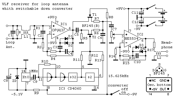
Schematic:
Parts list:
| R
see text
R1,R2 100 W R3 470 W R4 10 kW R5 1 kW R6 2.2 kW R7 1 kW R8 100 kW R9 see text R10 100 kW R11,R12,R13 10 kW R14 100 W R15 22 kW R16 220 W R17 47 W |
P
20 kW,
log.
C1
see text
L1,L2 see text |
T1,T2
BF 245(B)
D1,D2 shottky (BAT...) D3,D4 1N4148 ZD zener diode 5.1V IC1
OP37 / OPA37
connectors for
|
Description:
The circuit is powered from two batteries of 9V each for positive and negative supply.
C1 can be selected to make a resonance with the loop's inductance at the frequency of interrest. I suggest to select R ( a few ohms only) so that Q is not bigger than 4, this makes tuning uncritical enough for mobile use. L1 is inserted to prevent RF current caused by nearby radio stations to flow into the receivers input. Otherwise you will very likely listen to a commercial radio program in stead of what you want to get. L1 can be any usual RF suppression coil with two windings on a toroid core. C2 servers the same purpose. R1 supresses unwanted RF resonances with L1-C2 and also assures stable operation at high impedance with the antenna resonant circuit or even open input terminals.
The OP37 / OPA37 is chosen for its low noise contribution, high bandwidth, good availability and moderate price. The amplification is determined by R4/R2 an set to 100. C4-R3 reduces gain with frequencies above 50kHz and allows for stronger negative feedback with higher frequencies in order to avoid demodulation of RF. D1-D2-C3 will limit the amplitudes of short strong pulses from nearby spherics or switching events at nearby power lines. This part can be omitted at will.
When the switch is turned off, T1 is in conductive state and the signal reaches the potentiometer for loudness without relevant attenuation.
The NE5534 is chosen for moderate low noise and high bandwidth. Gain ist set to 220 with this stage. The additional network for negative works similar as in the first stage and may not be omitted: D3-D4 will limit the output amplitude to a value far below the capabilities of the amplifier, thus allowing to drive a load of low impedance compared to the specifications for the chip. This limitation also serves for ear protection while listening to weak signals among loud spherics. L2 again prevents RF current to flow through the unit and makes the headphone or whatever you will connect to the output not work as an antenna for disturbing RF reception.
The frequency response of this antenna/amplifier combination exhibits a gain that is increasing linear with frequency. This helps to suppress powergrid hum and intensifies the signals from VLF radio stations. As sperics are also intensified, the limitation of amplitide becomes very valuable. The high gain of the amplifier in non converting mode may cause an oscillation due to magnetic feedback from a headphone to the loop antenna, so keep those parts in a good distance.
When the switch is closed, the circuit is in converter mode: The signal path along T1 is turned off and C5-R5 act as a high pass filter that further attenuates signal with frequencies below 10 kHz. Simultaneously the crystal oscillator generates a clock signal for the sequencing counter / frequency divider. This chain genaretes an output frequency of 15.625 kHz, wich is exactly the video line frequency for european TV. The frequency is chosen in order to avoid artificial disturbing signals from neighbors who are watching TV. I do not know which frequency is used in the US. R9 must be selected as great as possible so that the voltage at C8 does not fall below 4.7 V when the battery voltage drops down to 7V. With the signal generated so far there is added another one of double frequency. Thus we obtain shorter pulses switching T2 to conductive state. The pulsating resistance of the FET's channel makes this stage act as a mixer producing the difference frequency from the input signal and the oscillator's signal. In the case of Grimeton this is 1.575 kHz. R7-C7 act as a low pass filter that attenuates everything above 3 kHz, a duty/cycle of 1/4 is considered for selection of R6. With T1 and T2 it makes no difference which is source and drain.
This article is intended to be republished
at VLF OPEN LAB with an added report of
experience later.