
Ultra Low Power
ELF/VLF Receiver Project
 |
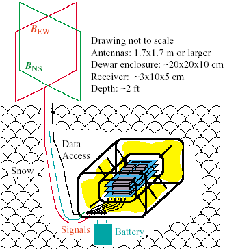
Fig. 1. Ultra-low-powerELF/VLFreceiver system for use in polar regions. Depicted here is a single autonomous system, enclosed in a dewar (for temperature control) and buried ~2 to 3 ft deep in the snow immediately underneath the sensors, which consist of two crossed magnetic loop antennas. The ultra-low-power ELF/VLF receiver system consists of several Application Specific Integrated Circuit (ASIC) chips, which together with associated external circuitry and nonvolatile memory, fits into an enclosure no larger than a single paperback book, and operates continuously while consuming only a total of ~10 milliwatts. At the same time, the new receiver is much lower cost (<$2000 per unit, including antennas and battery), much more robust and easy to duplicate (due to integrated design and much fewer components), and has many times the capability and flexibility of previous systems, in terms of bandwidth and programmable on-board DSP processing power. |
|
Fig. 2. Stanford ELF/VLF receiver at an unmanned AGO site. This system, currently operational at five different remote high latitude Antarctic sites [Salvati et al., 1999], was designed and build in 1990 specifically for use in unmanned sites, with minimal power demands on power. It consists of a magnetic loop antenna (either a 1.7x1.7m or 4.9x4.9m square – both shown in the photo above) connected to a preamplifier (grey box with sealed lid shown in lower left) buried immediately underneath, which is powered by and sends data over a~500 ft coaxial cable (shown rolled up) to the station (shown in upper left), in which resides the main receiver unit (the box with the blue front panel) consisting of a line receiver, various fixed band filter channels, and a broadband snapshot system, as depicted in the block diagram. This ‘low power’ ELF/VLF system specially designed for unmanned sites with limited power nevertheless consumes ~6 to 7W, depending on operational modes. The ultra-low-power ELF/VLF receiver system will provide the same functionality at a power level of ~10 mW, while eliminating the need for the preamp, and the cable, and reducing the physical size of the main receiver unit to a housing as large as a small paperback book, and allowing for substantial enhanced flexibility (e.g., bandwidth and channel selection under software control) of operation.
|
|
|
|
Fig. 3. The cusp lab at South Pole. Parts of the ELF/VLF Receiver equipment currently in use are shown. The PC computer which does the A/D conversion is now shown. Similar systems are also in operation at Palmer and McMurdo Stations, Antarctica, and in Greenland (at Thule and Sondrestromfjord). |
|
Fig. 4. ELF/VLF observation sites. Marked in red are manned and unmanned sites operated by the United States, while those sites marked in green are operated by the British Antarctic Survey. Stanford University ELF/VLF receivers are currently deployed at South Pole (SP) and Palmer (PA), as well as at the AGO sites P1, P2, P3,P4, and P5.
|
|
|
|
Fig. 5. ELF/VLF chorus emissions observed at P2, Antarctica. The top panels show 2-sec snapshots illustrating the characteristic frequency-time signatures of rising chorus emissions. The lower panels show continous records of signal amplitude in selected narrow bands, illustrating the characteristic morning local time (magnetic noon is approximately 1500 UT) peak in chorus activity. Simultaneous acquisition of the narrowband data and wideband spectral snapshots represent the typical targeted data acquisition strategies that would be used with the ultra-low-power ELF/VLF receiver. |
|
We now provide brief background on one particular type of plasma wave, namely discrete ELF/VLF chorus emissions. ELF/VLF chorus, named for its charactericstic sequence of repeating, usually rising and often overlapping coherent tones, ranks as the most intense of all naturally generated plasma wave emissions observed in the Earth’s magnetosphere, occurring regularly in association with disturbed magnetospheric conditions and seen frequently in association with microburst electron precipitation [e.g., Rosenberg et al., 1981] and other auroral activity. The onset time of growth of chorus has in past work been associated with arrival of magnetic disturbances [Gail and Inan, 1990]. However, the nature of such association has in general been complex and variable from event to event. More recently, a much more direct association of chorus onset and turn-off with sudden fluctuations in solar wind dynamic pressure and southward turnings of the IMF have been observed, both in situ [Lauben et al., 1998] and on the ground [Salvati et al., 2000]. The ground-based observation is particularly exciting, since the relationship between the solar wind and this dominant plasma wave emission can be continuously monitored. Understanding the circumstances of that are conducive to the generation of these intense emissions is important especially in view of the dominant nature of chorus in terms of its intensity and its known effects as the driver of energetic electron precipitation, pulsating aurorae, and maybe even the morningside diffuse aurora [Inan et al., 1992].
|
|
|
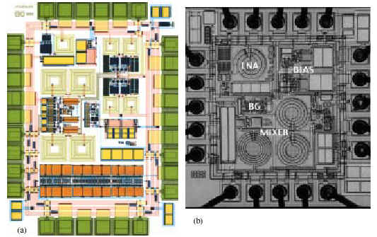 |
Fig. 7. 2-GHz single-chip radio developed at Stanford. (a) Layout of the 2 GHz, Integrated Front End CAD Tool layout specifying the design of an integrated LNA, with a Gilbert Cell mixer at 1.6 GHz. This design is optimized to match the impedance of a 50 ohm input to the LNA. The LNA is further designed to have a current density in transistor gate elements that produces the lowest noise figure for the CMOS technology. This is a noise figure of 1.1 dB. (b) Die Photo of 2 GHz Receiver Front End Photograph of a working chip fabricated at Maxim, Inc., incorporating the design shown in (a). Shown here is the LNA, with a noise figure of 1.2 dB, at 1.6 GHz, and a mixing stage that consists of a Gilbert Cell mixer with a noise figure of 6 dB. The mixer has a gain stage of 10 dB so that the combined noise figure of the receiver is 1.3 dB.
|
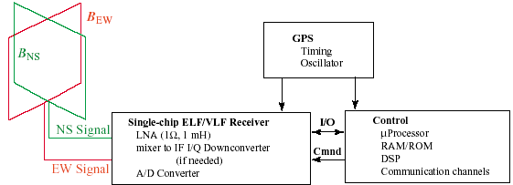 |
Fig. 8. Block diagram of the ultra-low-power ELF/VLF receiver. Schematic combining the single chip receiver with the single chip receiver and frequency reference oscillator and microprocessor and DSP control.
|
|
Antenna Impedance Match and Receiver SensitivityThe ELF/VLF antenna has an input impedance consisting of a 1 mH inductance in series with a 1 .resistance. Generally, matching the antenna impedance to the input impedance of a low noise amplifier (LNA) often means sacrificing sensitivity because of the difficulty of simultaneously optimizing both the matching impedance and the noise figure of the amplifier. For example, the minimum noise figure of a good LNA might be 1 dB, with the LNA at room temperature and matched to an impedance that has the lowest noise figure. When matched instead to the impedance of an antenna, the LNA noise figure typically increases to 3 dB. However, discussed in the previous section, the Stanford ULP group has had recent success at RF frequencies in simultaneously optimizing the LNA for both matching the antenna impedance and minimizing the noise figure for a single chip receiver. In this case, antenna impedance depends on device size while noise figure was discovered to depend on device current density. Since device size and device current density are independant characteristics in an integrated circuit, they can be simultaneously optimized. When this optimization was performed, a noise figure of 1.1 dB was obtained for an LNA in a BiCMOs integrated circuit that was closely matched to the antenna impedance, with the design shown in Figure 7.
At VLF frequencies, good receivers have a noise figure close to 3 dB, while the LNA in those receivers have a noise figure closer to 1 dB. A similar opportunity is to reduce the receiver noise figure by optimizing the noise figure and the impedance match. We will to integrate the VLF receiver front end components in a single CMOS chip. By integrating the receiver components, the LNA will be implemented in CMOS. Although CMOS devices tend to have higher noise figures than, for example devices in bipolar technology, the trend to small device size offsets this difference to where CMOS devices now have noise figures of ~2 dB. Thus, integrating an ELF/VLF receiver in CMOS can produceperformance that is at least as good as the current discrete component implementations. We further will investigate the attractive prospect that the receiver noise figure can be improved through the process of simultaneous optimization of the impedance match and noise figure minimization. New elements appear in adapting the method from RF to the VLF and promise insight into the behavior of low frequency amplifiers. For example, the low, almost purely reactive impedance of the VLF antenna, together with 1 /f character of noise at VLF frequencies differs from the 50 ohm, resistive impedanceand white noise distribution at higher radio frequencies. We will incorporate these differences in a fresh approach that simultaneously optimizes the impedance matching while minimizing the noise figure of the receiver.
Stable Time and Frequency ReferenceThe VLF receiver incorporates a miniature GPS receiver as the source of a stable time and frequency reference. The power and size of GPS receivers has been shrinking rapidly, however a large gap still remains between the ~100 mW chips now available and the ~10 mW goal of theultra-low-power ELF/VLF receiver. To mitigate this discrepancy, we are to achieve the ~1 µsectime resolution needed in an ELF/VLF receiver (note that the maximum bandwidth is 100 kHz so that 1 µsec resolution is well enough) by using the GPS receiver only occasionally, for example once ortwice per day, to synchronize a thermally isolated crystal resonator which is then the source for a timing generator and frequency reference. A thermally isolated, good quality crystal resonator has an Allen Deviation of typically better than 10 -10, for 1000 to 10,000 sec, which is about ~1 µsec/day. The driftdue to aging is larger, about ~10 µsec/day. By synchronizing to GPS once or twice per day, the effects ofdrift and variation could easily be compensated to the precision needed by the ELF/VLF receiver. GPS satellite lock is achieved generally in at most ~1 minute, so that the duty cycle of the GPS receiver wouldbe 2 minutes every 24 hours, so that a ~100 mW GPS card would only consume an average power of~ 0.1 mW, well within the 10 mW average consumption of the ELF/VLF receiver system.
Data StorageThe technology in FLASH memory has been leapfrogging its capacities with no sign of slowing down. Present, commercially available memories have up to 64 Mbyte capacities, (see e.g. 16Mx8, Samsung K9F2808U0M, 32Mx8 Toshiba TC58256FT, and 64Mx8 Toshiba TC58512FT) and a handful of these chips would have the capacity to store 1 Gbyte of data. The great advantage of FLASH memory is retention at zero power. The power used by these memories in writing to them is dependent on data rates, so that for the small few kHz bandwidths of ELF/VLF applications only ~1 mW is needed. Atsubstantially higher data rates some compaction, or data compression would be necesssary. As part of our development we will evaluate methods of compression and data abstraction using the DSP capabilities of the receiver to optimize the power allocation between the signal processing and memory transactions.
When used at AGOs or manned stations, the data from the ultra-low-power receiver can be brought back to the station over a serial data line or an optical fiber as discussed in Sections B.1 and B.2. Our preliminary investigations of optical fiber links indicate that translators between twisted pair and ~2 kmfiber optic link are commercially available (e.g., Telebyte Model 373) and that the relatively low data transmission rates ( <1 Mbits/s) required for the ELF/VLF aplication in hand can be easily accomodatedwithin a 10 mW power budget. As we investigate these possibilities, we expect to significantly benefit from discussions with Professor Leonid Kazovsky of Star Lab, an expert in optical fiber technology.
Digital Signal ProcessorsThe announcement of comercially available very low power DSPs, (see e.g. TI TMS320LC545, and TMS320C55x core), with power vs performancee in the range of 0.25 mW/MHz down to 0.05 mW/MHz, opens the door to using DSP in a miniaturized VLF receiver operating at 10 mW. In addition, work in the ULP group in STAR Lab has produced an ultra-low-power FFT processor with the lowest power benchmark which has already been fabricated and is referred to as the SPIFFIE chip [ Baas, 1999].SPIFFIE is a 1024-point single-chip FFT processor designed for low power operation, operating at a clock rate of 80 MHz, providing a 1024-point FFT every 60 microseconds while consuming only ~8mW. This performance represents an energy efficiency of over 75 times better than any previous FFT processor. By evaluating both commercially availiable DSP units and the continued development of ULP DSP systems a digital signal processing capability can be included in the ELF/VLF receiver within the power/performance goals.
Thermal Insulation of the Receiver SystemThe ultra low power consumption of the ELF/VLF receiver provides a particular challenge when deployed for use in cold polar region environments (e.g., the Antarctic plateau) where the outside temperature may vary between -80.C to +30. C. ELF/VLF preamplifiers currently in use (see the graybox in Figure 2) are typically buried in ~2 ft of snow, so that they remain nearly uniformly at about- 50. C but are kept at acceptable temperatures (-10.C to +20. C) by the heat dissipation of their ownelectronics. At a power level of only ~10 mW, the system cannot be kept in this temperaturerange, without a more sophisticated thermal enclosure.
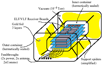
In this connection, we have consulted Professor R. Moffat of the Mechanical Engineering department of Stanford, who is a world reknown expert in heat transfer, insulation and electronics cooling. A preliminary design of a thermal insulation dewar by Prof. Moffat is shown in Figure 9 and briefly described below.
The system consists of two small, rectangular, stainless steel capsules, one inside the other. The inner one containing the ELF/VLF receiver and nonvolatile (flash) memory boards. Both are hermetically sealed. Lead wires (6 are shown) stick out of one end of the inner capsule through gas tight seals. This is important because they have to hold a fairly good vacuum in the space around this capsule. Any volatile products that outgas from the receiver or its extension wires (or their insulation) will rapidly raise the pressure in the supposed vacuum space. An increase in pressure will increase the heat loss to an unacceptable level. The recommended pressure is 310 -4 Torr in the chamber. The inner containeris suspended inside the outer capsule by its own lead wires, aided by some sort of a spider like, low conductivity structure that is slipped into the system. It should not be pressed tightly in, since that would increase its heat loss capability. Gold foil of at least 50 µm thickness should be wrapped loosely aroundthe inner container, and also fitted loosely around the inside of the outer pressure vessel. A third layer of foil should be "built in" to the spider-like positioning and supporting structure. These three layers of gold will reduce the radiant heat loss to a very low value. If the pressure inside the pressure vessel can be kept below 310 -4 Torr, the total heat loss should be less than ~10 mW watt in a -50. C environment,and thus the VLF receivercan be kept at a temperature in the range of -10. C to +20. C. The pressureinside the inner container is not important, hovever it must not leak. To acommodate a small amount of outgassing a ’getter’ will be mounted in the vacuum space.
The dewar design will be further optimized during the development effort, which Professor Moffat will participate as a Co-Investigator. Several dewar designs will be tested in the thermal insulation laboratory facilities of Prof. Moffat’s research group, with an eye on the desire to keep the cost of the dewar low, so that the total cost of an ultra-low-power ELF/VLF receiver together with antennas, battery, and the dewar is ultimately <$2000.
|
|
Fig. 9. Thermal isolation dewar for the ultra-low-power ELF/VLF Receiver. Design consists of two hermetically sealed containers. Inner container encloses the VLF receiver pc boards, and is suspended inside the outer container by a spider filament network. One, or more layers of gold foil line the inside of the outer container to increase the thermal insulation. The outer container is hermetically sealed as well and is evacuated to a pressure of 10-4 torr. Six vacuum sealed feed-throughs allow electrical connection to the inside VLF receiv er electronics.
|
 |
|
BatteriesWith a total continuous power consumption of only ~10 mW, the ELF/VLF receiver systemcan be ideally powered by batteries, even when used at an AGO or manned site. For this purpose, we are to investigate the potential use of batteries produced by Hawker, Inc., which are currently used in Antarctica. Our preliminary investigation indicates that their Cyclon series of the Hawker batteries works down to -65. C. To supply ~10 mW for one year, we need to more than 10 amp-hours. Thebattery performance at -50. C is equal to 25% of its room temperature capacity. The Hawker J-cellspecifications, in the Cyclon series, is 8 A-hr, at 2 V, in an approximately 5 cm diameter, 14 cm high, rigid plastic container that weighs 840 gm. To run a 10 mW, VLF receiver at 2V, for a year, would require 16 to 20 J-cells in parallel, assuming the batteries were buried in the snow at an ambient temberatureof -50 C. The batteries would then weigh ~17 kg. The dewar containing the VLF receiver could be placedinside the battery cluster to provide an a bit of extra thermal protection and simple access. |
|
|
Last Updated: June 2001.