Experiment about the Gilbert cell double balanced mixer.
It may be the spell miss of the Gilbert cell double balanced mixer. I know
the name only in Japanese. I have used this type of circuit as the IC.
TA7320 and TA7310 are the Gilbert cell double balanced mixer made by Toshiba
company. It is famous as MC1496 or SN76514 in U,S,A. I used them as a black
box for many years. But in these days my inter net friend taught me that
this circuit is based on the differential amplifier. I made some experiment
about this circuit. And I feel that I could understand how it works.
gil2.gif

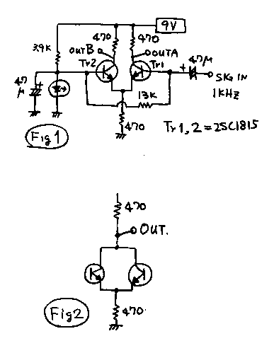
See the figure 1! This is the differential amplifier. The transistor1 works
as a emitter grounded amplifier. Therefore on the OUTA port ,there comes
the inverted phase signal of the input. The transistor2 works as a base
grounded amplifier. Therefore on the OUTB port ,there comes the non inverted
phase signal of the input. When I input the 40mVc-p (Center to Peak) 1kHz
signal on the SIG IN port , both amplitude of the output ports were 300mVc-p.
Therefore when I connected the OUTA port with OUTB like the figure2, very
small signal (10mVc-p) became on the OUT port. The inverted signal of the
OUTA might have canceled the non inverted signal on the OUTB port. This
type of mixer was used on the ancient tube receiver with 12AU7 named tube.
gil3.gif

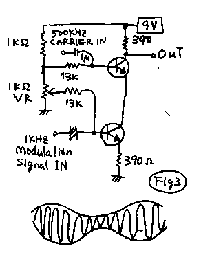
As a next experiment , I made tohempole mixer. See the figure3! With inputting
the modulation signal on the downside transistor, the carrier signal of
the upper side transistor was modulated by the modulation signal. I can
watched the amplitude modulated signal on the OUT port on the cathode ray
tube of my oscilloscope. I had to tune the bias control potentio meter
"variable resister" to get such a beautiful signal. On the Gilbert
cell , basic theory of it*s modulator based on this figure. Lower side
transistor modulates the upper side transistor. But on the Gilbert cell,
the carrier signal itself do not came on the output port. Also, the modulation
signal itself do not came on the output port. Both basic signals were canceled
by the circuit. I will explain how it works, how the Gilbert cell cancels
the carrier signal and modulation signal.
gil4gif

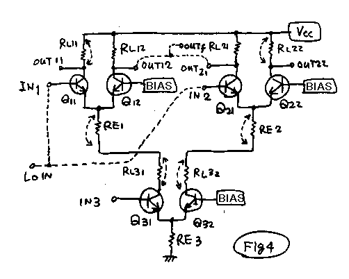
See figure 4! Three differential amplifiers are connected. I named all
the transistors and resisters as this figure. Connect IN1 and IN2! I named
it as LOIN " Local oscillator input". Connect OUT12 with OUT21
port! I named it as OUTf " out final". The modulation signal
put on the IN3 port produces inverted current on RL31 resister. This current
is divided for Q11 and Q12. And this current flows on the RL12 resistor.
On the other hand, the modulation signal put on the IN3 port produces "non"
inverted current on RL32 resister. This current is divided for Q21 and
Q22. And this current flows on the RL21 resistor. Therefore , the modulation
signal do not came out on the OUTf port , as the result of canceling of
the two currents. The carrier signal input on IN1 port produces non inverted
signal on the OUT12 port, because Q12 works as the differential amplifier.
The carrier signal input on IN2 port produces inverted signal on the OUT21
port, because Q21 works as the emitter grounded amplifier. Therefore ,
the carrier signal do not came out on the OUTf port , as the result of
canceling of the two currents. In order to complete this circuit, please
short the useless resisters! The name of the useless resisters are R11,R22,
RE1,RE2,RL31,RL32. You can understand this circuit is the famous Gilbert
cell. Rechte gemacht!
gil5.gif

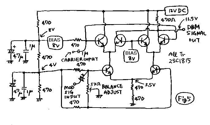
I felt that I could understand the Gilbert cell. In order to complete this
experiment, I made this circuit on the discrete board. All the transistors
are 2SC1815-Y. I do not know they may be the same lot. But I bought them
on the same package "1500 yens with 200 pieces". I did not feel
so happy when I turn on the power switch. Because it produced the beautiful
doubly balanced signal in instantly, as it indicated " you can see"
on the picture. But I felt a small happiness when I tuned the balance adjust
resister. The carrier null point was different from the modulation signal
null point.
gilph.gif

The performance of the circuit indicated on the figure 5.
The Carrier was 7-mVc-p 500kHz.
Modulation signal
(mc-p) |
Output signal
(mVc-p) |
Gain(dB) |
Carrier suppression
(dB) |
| 0 |
10 |
- |
0 |
| 10 |
70 |
16.9 |
-17 |
| 20 |
170 |
18.5 |
-25 |
| 30 |
220 |
17.3 |
-27 |
| 38 |
270 |
17.0 |
-29 |
Kazuhiro*s cell -----add description on 23 Jan 2000
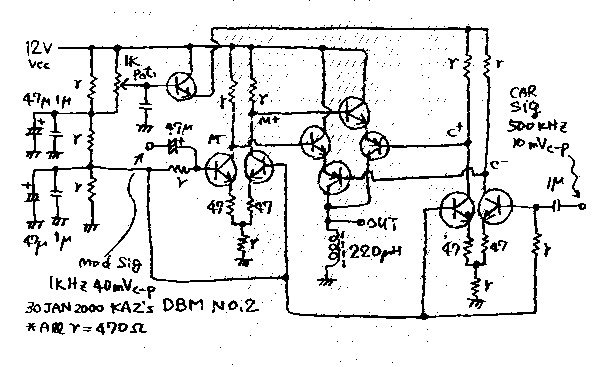
I tried to make a new circuit to act as a double balanced mixer like a
Dilbert cell. My American friend taught me that the name what I say may
be "Dilbert". But I already named this page as "gil. Html".
To change the name of the page is very difficult for me HIHI.****Description
add on 2 May2001***Japanese electric magazine named for " Transistor
technology" on May 2001 introduced us the developer of this circuit
as Mr.Barrie Gilgert with his photo. He is a Manager in Analogue devices
Co. ******
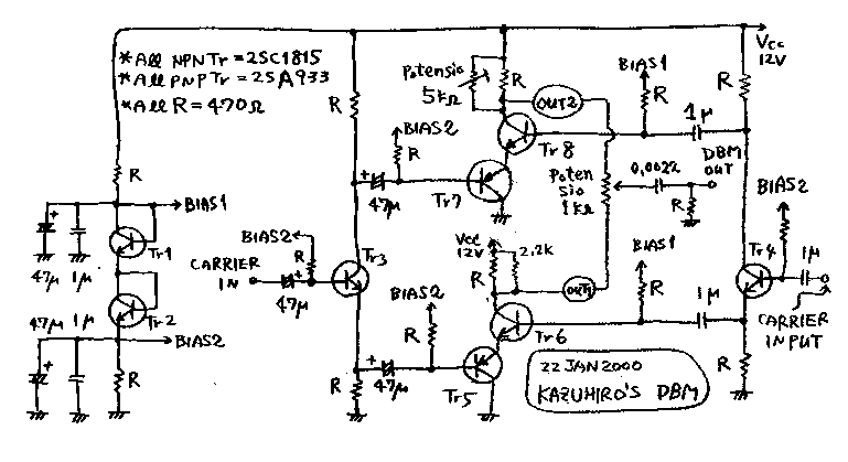
1. As a first basic part of double balanced mixer , I made a phase inverter
of the modulating signal. For this purpose, Dilbert uses a differential
amplifier. I use an collector emitter divider , like a plate cathode divider
of the Williamson amplifier. See fig7! The transistor named Tr3 works for
this purpose.
2. As a second basic part of double balanced mixer , I made a phase inverter
of a carrier signal. Dilbert uses a differential amplifier also for this
purpose. I use an collector emitter divider also for this purpose. See
fig7! The transistor named Tr4 works for this purpose.
3. As a third basic part of double balanced mixer , I made a mixer. For
this purpose, Dilbert uses a NPN NPN totem pole. I use an emitter connected
NPN PNP totem pole for this purpose. See fig7! The transistor named Tr5
and 6 work for this purpose. This part makes an amplitude modulated high
frequency signal.
4. As a fourth basic part of double balanced mixer, the same type mixer
must be made as a last one. But for this mixer, the inverted modulating
signal and the inverted carrier signal must be used. Frankly to say, I
did not want to use the capacitor for connecting this mixer with the twin
divider. I wanted to connect them directly. But I cannot develop any bias
system to joint them directly.
5. As the end of the double balanced mixer, twin amplitude modulated signals
must be combined. See fig7! The potensio meter 1k ohm works for this purpose.
This part makes an double side band signal from a pair of AM signals. The
potensio meter must be tuned to make minimize a leak of the carrier signal
500kHz on the OUT port. You can see the 0.0022 micro farads capacitor and
R= 470 ohms resistor near the OUT port. It is a high pass filter to reject
a modulating signal on the OUT port.
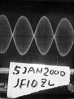
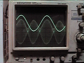
You can see the photo 2. The carrier suppression is not so good as the
Dilbert's cell. I will write the total performance on the same time as
I got this photograph.
Modulating signal: 1kHz, 30mVc-p
Carrier signal: 500kHz, 7mVc-p
Output signal: 30mVc-p
Carrier leak : 6mVc-p
Carrier suppression: -13dB
You may be able to construct some kind of double balanced mixer circuit.
You will be able to use a dual gated FET on the mixer. You will be able
to use a wide band transformer made with ferrite beads for the phase inverter.
The total performance will be great or poor, depending on which type of
circuit do you choose. Isn't it joyful to think about such a new circuit?
gil7.gif

gilph2.gif : Uppersign wave is a modulating signal 1kHz. The lower signal
is DSB signal.

gil8.gif

30Jan2000***discription add about the experiment of differential amplifier
and the modification of Kaz's double balanced mixer
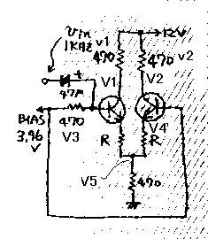
1. the experiment of differential amplifier
I learned on the Motorola data book about MC1496 that the gain of the Dilbert
cell can be changed by the external resister of the emitter. And I thaught
that this resister may be able to adjust the current balance of the differential
amplifier. See fig8! I put the two resisters on the emitter of the differential
amplifier. I learned how these resistors works. See the data table.
***V1=voltage of the collector of left transistor.
***V2=voltage of the collector of right transistor.
***V3=voltage of the common resister.
***V4=voltage of the emitter of left transistor.
***V5=voltage of the emitter of right transistor.
***dV=V1-V1 (difference of collector voltage)
***n=dV/(Vcc-V1)*100% (difference percentage of collector voltage) ***vin=50mVc-p
constant modulating signal 1kHz
***v1=signal of the collector of left transistor.
***v2=signal of the collector of right transistor.
***dv=v1-v2(difference of collector signals)
***z=dv/v1*100%(difference percentage of collector signals)
***g=20log(v1/vin) (voltage gain of signal)
***rezult1:To improve the difference percentage of collector signals, R
must be about10% of the emitter common resister.
***result2: To improve the difference percentage of collector voltage,
R is the the bigger the better.
***result3: To get more gain , R is the smaller the better.
| R |
ohm |
0 |
4.7 |
22 |
47 |
210 |
| V1 |
DC volts |
10.80 |
10.63 |
10.53 |
10.54 |
10.67 |
| V2 |
DC volts |
9.97 |
10.15 |
10.29 |
10.37 |
10.64 |
| V3 |
DC volts |
3.37 |
3.26 |
3.20 |
3.13 |
2.69 |
| V4 |
DC volts |
3.37 |
3.27 |
3.26 |
3.27 |
3.25 |
| V5 |
DC volts |
3.37 |
3.37 |
3.32 |
3.28 |
3.26 |
| dV |
DC volts |
0.83 |
0.48 |
0.24 |
0.17 |
0.03 |
| n |
% |
69 |
35.0 |
16.3 |
11.6 |
2.25 |
| vin |
mVc-p |
50 |
50 |
50 |
50 |
50 |
| v1 |
mVc-p |
1.0 |
720 |
350 |
190 |
60 |
| v2 |
mVc-p |
1.1 |
750 |
350 |
190 |
45 |
| dv |
mVc-p |
0.1 |
30 |
0 |
0 |
15 |
| z |
% |
10 |
4.1 |
0 |
0 |
25 |
| g |
dB |
26 |
23.2 |
16.9 |
11.6 |
1.5 |
gil9.gif

2. the modification of Kaz's double balanced mixer By using modified differential
amplifier, I made the modified double balanced mixer. See the fig9! I show
you the total performance of it.
Modulating signal: 1kHz, 40mVc-p
Carrier signal: 500kHz, 10mVc-p
Output signal: 2000mVc-p
Carrier leak : 120mVc-p
Carrier suppression: -24dB
gil10.gif

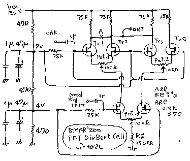
8Mar2000***discription add about the experiment of differential amplifier
."Double balanced mixer made with FET"
See the upper circuit! I have already enjoyed to make experiment about
DBM for this three month. I wrote 3 notebooks about it. I will show you
the double balanced mixer made with FET*s.
The performance of it is as follows.
Carrier signal: 100kHz, 400mVp-p
Output signal: 550mVp-p
Carrier leak : non ,but double frequency of carrier signal leaks 50mVp-p
How to tune this circuit
1.Cut A point !
2.Omit the carrier! Input only the modulating signal! Tune pot 1 to balance
the signal of drain of Tr1 and Tr2!
3. Tune pot 2 to balance the signal of drain of Tr3 and Tr4!
4. Tune pot 3 to balance the signal of drain of Tr1 and Tr3!
5. Connect A point! And input the carrier!
Comment
1. To make a good differential amplifier with FET, The higher gm the better.
The FET 2SK372 has 60mS as it*s gm.
2. To make a good differential amplifier with FET, The higher the soace
resister the better.
3. I did not get the pare tubes for this gear, I must make balance one
by one.
gil11.gif*****fig11.

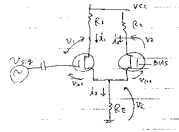
Description add on 30 Mar 2000***** Calculation of signal balance of differential
amplifier made by FET.
In order to make a good carrier suppression with the Dirbert cell, I must
make good balanced differential amplifier with FET. In order to make good
differential amplifier, I must use big gm FET. And also I must use big
resister for the source. I learned them from experiment. But I did not
understand the reason. I made calculation about the signal balance of differential
amplifier to understand the reason. See fig11!
v1: the signal out on the drain of left FET
i1:signal current on the drain of left FET
vin1: the signal input of left FET= voltage between the gate and source
gm1:Conductance of left FET
i1=gm1*vin1....................(1)
v2: the signal out on the drain of right FET
i2:signal current on the drain of right FET
vin2: the signal input of right FET= voltage between the gate and source
gm2:Conductance of right FET
i2=gm2*vin2....................(2)
i3=i1+i2................................(3)
ve: voltage of source is decided by the current flows on Re resister
ve=i3*Re..............................(4)
vsig: signal voltage on the gate of the right side are sum up of ve and
vin1
vsig=ve+vin1........................(5)
The gate of the right side FET is fixed by bias voltage.
vbias=ve+vin2=0..................(6)
v1: signal voltage of the drain of the left FET is culculated by the current
of drain resistor.
v1=-R1*i1.............................(7)
About the right FET, the same way.
V2=-R2*i2...............................(8)
All the actors are on the stage now.
(1) ,(2).....to (3)
i3=vin*gm1+vin2*gm2..........(9)
(9) ......to (4)
ve=( vin*gm1+vin2*gm2)*Re.....(10)
from (6)
ve=-vin2...............................(11)
(11) ....to (5)
vin1-vin2=vsig.....................(12)
(11) .....to(10)
-vin2=(vin1*gm1+vin2*gm2)*Re.......(13)
from (12)
vin1=vsig+vin2...................(14)
(14) ....to(13)
-vin2=( (vsig+vin2)*gm1+vin2*gm2)*Re
-vin2=vsig*gm1*R1+vin2*gm1Re+vin2*gm2*Re
-(1+gm1*Re+gm2*Re)*vin2=vsig*gm1*Re
Therefore
vin2=-vsig*gm1*Re/(1+gm1*Re+gm2+Re)....(15)
(15) ....to(14)
vin1=(1+gm2Re)/(1+gm1*Re+gm2*Re)........(16)
From (7),(8)
v2/v1=R2*i2/R1*i1................(17)
(1) ,(2)....to(17)
v2/v1=R2*vin2*gm2/R1*vin1*gm1.............(18)
(15) ,(16)....to(18)
v2/v1=-R2*gm2*Re/R1*(1+gm2*Re)...........(19)
What I say from the (19)....1
If "gm*Re" is big enough than 1 , v1 and v2 become the same signal
width. But in actual FET , gm = 10m mho, Re= 100 ohm. Therefore gm*Re=1.
What I say from the (19)....2
Anyway v2 must be smaller than v1.
What I say from the (19)....3
To get big "gm*Re" , we must use big bias voltage , and to use
the FET with bigger Re resister.
僊儖僶乕僩僙儖宆僟僽儖僶儔儞僗僪儈僋僒乕乮埲壓俢俛俵乯偺帋嶌偲幚尡乮俆俰俙俶乫侽侽乯
巹偑丄弶傔偰傾儅僠儏傾柍慄壠偲偟偰丄偄傢備傞揹榖偺岎怣偵惉岟偟偨偺偼丄暿偺儁乕僕偱徯夘偟偰偁傞乽俀侾俵俫倸俢俽俛憲怣婡乿偱偟偨丅偙偺憲怣婡偵偼丄俿俙俈俁俀侽俹偲偄偆俬俠幃偺俢俛俵傪巊偭偰偄傑偟偨丅偦偺惢嶌偵偁偨偭偰偼丄俈侽侽侽墌偱攦偭偨搶幣偺俬俠偺僨乕僞僽僢僋偺拞偵丄俿俙俈俁俀侽俹偺摍壙夞楬偑昤偄偰偁傝傑偟偨偑丄摉帪偺巹偵偼偦偺夞楬偑側傫偺帠傗傜偝偭傁傝暘偐傝傑偣傫偱偟偨丅偦傟偱傕偦偺傑傑丄嶨帍偺夞楬椺偲摨偠條偵慻傫偩強丄摨偠條側攇宍偑僆僔儘偱娤嶡偱偒傞俢俽俛怣崋偑偊傜傟偨偺偱丄偦偺傑傑偢偭偲偙偺俬俠傪巊偭偰偒傑偟偨丅嵟嬤丄俰俙亅俻俼俹僋儔僽偺儊乕儖偺傗傝庢傝偺拞偱偙偺夞楬乮僊儖僶乕僩僙儖偲偄偆偦偆偱偡丅乯偺摦嶌偑榖戣偲側傝丄偙傟偑嶌摦憹暆婍傪婎杮偵偟偨夞楬偱偁傞帠偑傢偐傝傑偟偨偺偱丄偦傟偑乽堷偒嬥乿偲側偭偰丄偄偔傜偐偺幚尡傪峴偄丄偙偺夞楬偺帠偑巹側傝偵傢偐傝傑偟偨丅埲壓偵巹偺峴偭偨幚尡偲丄峫嶡傪徯夘偟偰丄偙偺夞楬偺夝愢傪偟偰傒傑偡丅偪傚偭偲傗傗偙偟偄榖偵側傝傑偡偑丄摢偺懱憖偩偲巚偭偰撉傫偱偔偩偝偄丅
gil2.gif

傑偢丄恾1偺夞楬傪慻傫偱傒傑偟偨丅偙傟偑嵎摦憹暆婍偺婎杮夞楬偱偡丅僩儔儞僕僗僞乕侾偼丄僄儈僢僞乕愙抧偲偟偰摦嶌偟偰偄傑偡丅儀乕僗偐傜擖椡偝傟偨丄掅廃攇怣崋乮偙偙偱偼丄帺嶌偺僂僀乕儞僽儕僢僕敪怳婍偱嶌偭偨侾倠俫倸係侽倣倁們乕倫偺掅廃攇怣崋傪巊偭偰幚尡偟偨丅乯偼丄俿倰侾偺僐儗僋僞乕偵俁侽侽倣倁們亅倫偺怣崋偲偟偰尰傟傑偡丅堦曽丄俿倰侾偼摨帪偵僄儈僢僞乕僼僅儘儚乕偲偟偰傕摦嶌偟偰偍傝丄僄儈僢僞乕偵傕擖椡怣崋偲摨偠戝偒偝偺怣崋偑丄侽丏俆儃儖僩偺尭嶼偝傟偨宍偱尰傟傑偡丅堦曽丄俿倰俀偼儀乕僗偑堦掕偺揹埵偱屌掕偝傟偰偄傑偡丅偙偺偨傔丄偙偺怣崋偼丄俿倰俀偵偲偭偰僄儈僢僞乕擖椡怣崋偲側傞偺偱丄俿倰俀偼丄儀乕僗愙抧憹暆婍偲偟偰摦嶌偟傑偡丅偙偺寢壥丄俷倀俿俙偵偼擖椡偲媡偺埵憡偺怣崋偑尰傟丄俷倀俿俛偵偼丄擖椡偲摨偠埵憡偺怣崋偑尰傟傑偡丅偳偪傜傕怳暆偼丄俁侽侽倣倁們乕倫偱偟偨丅
偦偙偱丄恾俀偺條偵丄俷倀俿俙偲俷倀俿俛傪捈愙偮側偄偱傒傞偲丄侾俉侽搙堎側傞怣崋偑偍屳偄偵懪偪徚偟偁偆偺偱丄俷倀俿偲帵偝傟偨弌椡抂巕偵偼丄摿偵怣崋偼弌偰棃傑偣傫偱偟偨丅偦傟偱傕椙偔尒偰傒傞偲侾侽倣倁偼弌偰偄傞偺偱丄偙偺夞楬傪憹暆婍偲偟偰曔傜偊偨応崌偺棙摼偼丄擖椡係侽倣倁偵懳偟偰丄弌椡侾侽倣倁偱偡偐傜丄乕侾俀倓俛偲偄偆帠偵側傝傑偡丅
gil3.gif

師偵丄恾俁偺夞楬傪慻傫偱丄曄挷偺幚尡傪偟偰傒傑偟偨丅忋懁偺僩儔儞僕僗僞乕偵僔僌僫儖僕僃僱儗乕僞乕偐傜俆侽侽倠俫倸偺怣崋傪擖傟偰丄壓懁偺僩儔儞僕僗僞乕偵偼掅廃攇敪怳婍偺俆侽侽倠俫倸偺怣崋傪偄傟偰傒傑偟偨丅擇偮偺怣崋偑崿偞偭偰丄弌椡偵偼恾3偺壓懁偵彂偄偰偁傞傛偆側丄僽儔僕儍乕偺條側攇宍偑娤嶡偝傟傑偟偨丅妋偐偵擇偮偺怣崋偺妡偗崌傢偣偑峴傢傟偰偄傑偡丅偨偩偟丄偙偆偄偆怣崋偑弌偰偔傞堊偵偼丄偐側傝旝柇偵侾倠僆乕儉偺敿屌掕掞峈傪挷愡偟側偔偰偼側傝傑偣傫偱偟偨丅偙偺夞楬偱偼丄壓懁偺僩儔儞僕僗僞乕偺揹棳偑曄壔偡傞帠偵傛偭偰丄忋懁偺僩儔儞僕僗僞乕偵偲偭偰偺僄儈僢僞婣娨検偑曄傢傞偨傔偵丄忋懁偺憹暆婍偺棙摼偑曄壔偡傞偲丄夝庍偱偒傞偲偍傕偄傑偡丅僊儖僶乕僩僙儖偵偍偄偰傕丄忋懁偺係屄偺僩儔儞僕僗僞乕偵偼斃憲攇傪拲擖偟丄壓偺俀屄偺僩儔儞僕僗僞乕偵偼曄挷攇傪拲擖偟偰偄傞偺偱丄婎杮偼偙偺恾俁偺夞楬偲摨偠偱偡丅偨偩丄堘偄偼丄僊儖僶乕僩僙儖偱偼丄弌椡抂巕偵偼曄挷攇傕斃憲攇傕弌偰偙側偄偱丄偦傟傜偺妡偗崌傢偣偺怣崋偩偗偑弌偰偔傞傛偆偵堊偭偰偄傞偲偄偆揰偱偡丅
gil4gif
 恾係傪尒偰偔偩偝偄丅偙偺恾偱丄側偤乽僊儖僶乕僩僙儖偱偼丄弌椡抂巕偵偼曄挷攇傕斃憲攇傕弌偰偙側偄乿偲偄偆帠傪愢柧偟傑偡丅偙偺恾偼丄愢柧梡偺恾偱幚嵺偙偺夞楬傪慻傫偩傢偗偱偼偁傝傑偣傫丅恾侾偺嵎摦憹暆婍傪俁屄暲傋偰偄傑偡丅壓偺侾偮偺嵎摦憹暆婍偺俀偮偺僐儗僋僞抂巕偺忋偵丄偦傟偧傟嵎摦憹暆婍傪忔偣偰偁傝傑偡丅偦傟偧傟偺慺巕偵偼恾偺傛偆偵柤慜傪傆傝傑偟偨丅僶僀傾僗夞楬偼徣棯偟偰偁傝傑偡丅偙偙偱偼丄慡偰偺僩儔儞僕僗僞乕偑揔摉側揹棳偱摦嶌偱偒傞傛偆偵僶僀傾僗偝傟偰偄傞偲偟偰榖傪偡偡傔傑偟傚偆丅師偵丄恾偺揰慄偱帵偟偨傛偆偵丄忋偺俀偮偺擖椡俬俶侾偲俬俶俀傪偮側偄偱丄偙傟偵怴偟偔俴俷俬俶偲柤慜傪偮偗傑偡丅傑偨丄弌椡俷倀俿侾俀偲俷倀俿俀侾傕偮側偄偱偟傑偄丄偙傟偵怴偟偔俷倀俿倖偲柤慜傪偮偗傑偡丅偙偺柤慜偼偙偙偱偺愢柧偺堊偵偮偗偨偩偗偱丄偨偄偟偨堄枴偼偁傝傑偣傫丅偦偟偰俴俷俬俶偵斃憲攇怣崋傪拲擖偟丄俬俶俁偵曄挷怣崋傪拲擖偟偨偲偟傑偡丅曄挷怣崋偼俼俴俁侾偵媡憡偱尰傟丄偙傟偺揹棳偼俻侾侾偲俻侾俀偵暘棳偝傟傞偺偱丄俼俴俁侾傪棳傟傞媡憡偺敿暘偑俼俴侾俀偵棳傟傞帠偵
側傝傑偡丅堦曽丄俻俁俀偼曄挷攇怣崋偺摨憡揹棳傪弌椡偡傞偺偱丄俼俴俁俀偵偼曄挷怣崋偺摨憢偺怣崋偑側偑傟傑偡丅偙偺敿暘偑俻俀侾傪捠偭偰俼俴俀侾偵尰傟傑偡丅偙偺寢壥丄俼俴侾俀偲俼俴俀侾偵偼偦傟偧傟媡憡偲摨憡偺怣崋偑弌偰偔傞偺偱丄偦傟傜偑憡嶦偝傟偰丄俷倀俿倖偲偟偰偼丄曄挷怣崋偼偱偰偒傑偣傫丅師偵丄斃憲攇怣崋偵娭偟偰愢柧偟傑偡丅俬俶侾偵報壛偝傟偨斃憲攇怣崋偼丄嵎摦憹暆婍偵傛偭偰摨憡憹暆偝傟偨怣崋偲偟偰俷倀俿侾俀偵弌偰偒傑偡丅堦曽丄俬俶俀偵報壛偝傟偨斃憲攇怣崋偼丄僄儈僢僞愙抧憹暆婍偲偟偰俻俀侾偑摦嶌偡傞偺偱丄俷倀俿俀侾偵偼丄媡憲怣崋偲側偭偰丄尰傟傑偡丅偙偙偱傕丄俷倀俿侾俀偲俷倀俿俀侾偼丄偦傟偧傟擖椡偝傟偨斃憲攇怣崋偵懳偟偰摨憡偲媡憡偺怣崋偲側傞偺偱丄偦傟傜傪偮側偘偰懌偟偁傢偣傞偲丄斃憲攇怣崋偼俷倀俿倖偵偼弌偰棃側偄帠偵側傞傢偗偱偡丅嵟屻偵丄偁傑傝堄枴偺側偄丄俼俴侾侾丆俼俴俀俀丄俼俤侾丆俼俤俀丆俼俴俁侾丆俼俴俁俀摍傪僔儑乕僩偟偰傗傟偽丄僊儖僶乕僩僙儖宆僟僽儕乕僶儔儞僗僪儈僉僒乕偺弌棃忋偑傝偱偡丅
gil5.gif

偲傑偁丄尨棟傪巻忋偱丄棟夝偟偨乮偮傕傝偵側偭偨乯偲偙傠偱丄恾俆偺夞楬傪幚嵺偵慻傫偱幚尡偟偰傒傑偟偨丅寢壥偼堦敪崌奿偱丄幨恀偺傛偆側傑偢傑偢偺摿惈偺俢俛俵偑弌棃傑偟偨丅斃憲攇傪俈侽倣倁堦掕偵偟偰丄曄挷攇傪挷惍偡傞偲丄栺侾俈倓俛偺棙摼偑偁傝傑偟偨丅儊乕僇乕偺惢昳偲摨偠偔傜偄偱偡丅嵟戝弌椡怳暆偼俀俈侽倣倁們亅倫傑偱妋擣偟傑偟偨偑丄傢偨偟偺帺嶌偺僂僀乕儞僽儕僢僕敪怳婍偱偼偙傟埲忋偺攇偑偩偣側偄偺偱丄偙傟埲忋偼妋擣偱偒傑偣傫偱偟偨丅傑偁廫暘偱偟傚偆丅偨偩偟丄僉儍儕傾僒僾儗僢僔儑儞偩偗偼丄儊乕僇乕惢偺暔偵媦傃傑偣傫偱偟偨丅恾偱乽俛俙俴俙俶俠俤俙俢俰倀俽俿乿偲彂偄偰偁傞丄暯峵挷惍梡偺俆倠僆乕儉偺敿屌掕掞峈傪挷惍偡傞偲丄僉儍儕傾嵟彫偵挷惍偱偒傞億僀儞僩偲丄曄挷怣崋偺捠傝敳偗偑嵟彫偵挷惍偱偒傞億僀儞僩偑暿側偺偑娤嶡偱偒傑偟偨丅偙傟偑側傫偲傕妝偟偄偱偡丅暯峵挷惍梡偺俆倠僆乕儉偺敿屌掕掞峈傪庢傝晅偗柍偄偲丄偝傜偵丄僉儍儕傾乕僒僾儗僢僔儑儞偑侾侽倓俛掱搙埆壔偟傑偡丅偙傟偱偼傕偼傗俢俛俵偲偼屇傋偨傕偺偱偼偁傝傑偣傫丅儊乕僇乕惢偺俬俠偱偼丄偙偙偼柍挷惍偱偡偐傜丄偝偡偑偵俬俠偼丄撪晹偺僩儔儞僕僗僞乕偑摨幙側偺偱偟傚
偆丅偪側傒偵丄偙偙偱偼僩儔儞僕僗僞乕偼慡偰俀俽俠侾俉侾俆偺倄偺摨偠戃偱俀侽侽屄傑偲傔攦偄偟偨暔傪丄柍嶌堊偱偮偐偭偰偄傑偡丅幚尡偭偰杮摉偵妝偟偄偱偡偹丅偦傟偠傖丅傑偨丅
gilph.gif

恾俆偺夞楬偺俢俛俵偲偟偰偺摿惈乮斃憲攇擖椡偼丄俈侽倣倁們亅倫堦掕乯
曄挷怣崋擖椡
乮倣倁們亅倫乯 |
弌椡乮倣倁們亅倫乯 |
棙摼乮倓俛乯 |
僉儍儕傾僒僾儗僢僔儑儞
乮倓俛乯 |
| 0 |
10 |
- |
0 |
| 10 |
70 |
16.9 |
-17 |
| 20 |
170 |
18.5 |
-25 |
| 30 |
220 |
17.3 |
-27 |
| 38 |
270 |
17.0 |
-29 |
乽嵒懞晽僊儖僶乕僩僙儖偺帋嶌乿捛壛婰嵹俀俀丏俰俙俶丏俀侽侽侽
僊儖僶乕僩僙儖偺尨棟丄摦嶌傪堦捠傝棟夝偟偨偺偱丄摨條偺僟僽儕乕僶儔儞僗僪儈僉僒乕傪暿偺夞楬偱巹側傝偵帋嶌偟偰傒傑偟偨丅扐偟丄僐僀儖傗僩儔儞僗偺椶偼巊傢側偄帠偲偟傑偡丅
侾丏 婎杮峔惉偦偺侾丗傑偢丄曄挷怣崋偱偁傞侾倠俫倸偺掅廃攇怣崋偐傜丄擖椡怣崋偵懳偟偰媡憡偲摨憡偺俀偮偺怣崋傪偮偔傝傑偡丅僊儖僶乕僩僙儖偱偼丄嵎摦憹暆婍偑偙傟傪峴偭偰偄傑偡丅傢偨偟偼丄懠偵埵憡斀揮傪峴偆夞楬偲偟偰丄俹俲暘妱乮僾儗乕僩丄僇僜乕僪暘妱乯夞楬偲偄偆偐丄僐儗僋僞丄僄儈僢僞暘妱夞楬傪巊梡偟傑偟偨丅恾俈偺俿倰俁偲昤偄偰偁傞僩儔儞僕僗僞乕偑丄偦偺巇帠傪偟偰偄傑偡丅
俀丏 婎杮峔惉偦偺俀丗師偵丄斃憲攇怣崋偱偁傞俆侽侽倠俫倸偺崅廃攇怣崋偐傜丄擖椡怣崋偵懳偟偰媡憡偲摨憡偺俀偮偺怣崋傪偮偔傝傑偡丅僊儖僶乕僩僙儖偱偼丄偙偙傕嵎摦憹暆婍偑偙傟傪峴偭偰偄傑偡丅傢偨偟偼丄偙偙偱傕丄僐儗僋僞丄僄儈僢僞暘妱夞楬傪巊梡偟傑偟偨丅恾俈偺俿倰係偲昤偄偰偁傞僩儔儞僕僗僞乕偑丄偦偺巇帠傪偟偰偄傑偡丅
俁丏 婎杮峔惉偦偺俁丗師偵丄曄挷怣崋偺摨憡怣崋偲丄斃憲攇怣崋偺摨憡怣崋偲偵傛偭偰丄怳暆曄挷傪峴偭偰丄怳暆曄挷攇乮偄傢備傞俙俵曄挷攇乯傪摼傑偡丅僊儖僶乕僩僙儖偱偼丄偙偙偱偼擇偮偺俶俹俶僩僞儞僕僗僞乕傪僩乕僥儉億乕儖愙懕偟丄巊梡偟偰偄傑偡丅傢偨偟偼丄俶俹俶僩儔儞僕僗僞乕偲俹俶俹僩儔儞僕僗僞乕傪僄儈僢僞乕嫟捠偱僩乕僥儉億乕儖愙懕偟丄巊梡偟偰偄傑偡丅恾俈偺俿倰俆偲俇偲昤偄偰偁傞僩儔儞僕僗僞乕偑丄偦偺巇帠傪偟偰偄傑偡丅
係丏 婎杮峔惉偦偺係丗師偵丄曄挷怣崋偺媡憡怣崋偲丄斃憲攇怣崋偺媡憡怣崋偲偵傛偭偰丄怳暆曄挷傪峴偭偰丄怳暆曄挷攇傪摼傑偡丅恾俈偺俿倰俈偲俉偲昤偄偰偁傞僩儔儞僕僗僞乕偑丄偦偺巇帠傪偟偰偄傑偡丅幚偼丄慡懱偺夞楬傪僐儞僨儞僒乕傪巊傢偢偵丄慡偰捈寢偟偨偐偭偨偺偱偡偑丄偙偺晹暘偵丄怣崋傪報壛偡傞堊偵偳偆偟偰傕僐儞僨儞僒乕傪巊傢偞傞傪摼傑偣傫偱偟偨丅偪傚偭偲巆擮偱偡丅
俆丏 婎杮峔惉偦偺俆丗忋偱嶌偭偨擇偮偺怳暆曄挷怣崋傪壛嶼偟偰俢俽俛怣崋傪摼傞丅偙傟偼丄壛嶼偲偄偭偰傕丄偮側偖偩偗偱偡丅恾俈偺俷倀俿侾偲俷倀俿俀偺娫傪傓偡傫偱偄傞侾倠僆乕儉偺億僥儞僔儑儊乕僞偱僶儔儞僗傪挷惍偟側偑傜丄壛嶼偟傑偡丅偦偺屻偺侽丏侽侽俀俀兪俥偺僐儞僨儞僒乕偲晧壸掞峈偱丄僴僀僷僗僼傿儖僞乕傪峔惉偟丄偙偙偵捠傝偸偗偰偔傞掅廃攇怣崋傪庢傝嫀偭偰偄傑偡丅偪傚偭偲偢傞偱偡偑姩曎偟偰偔偩偝偄丅寢壥偼壓偺幨恀俀偺擛偔丄傢偞傢偞斃憲攇挷惍傪庤摦偱峴偭偰偄傞偵傕娭傢傜偢偩偄傇梷埑斾偑傛傠偟偔偁傝傑偣傫丅偦傟偱傕偄偪偍偆俢俛俵偲偟偰摦嶌偼偟偰偄傞偺偱丄偙偙偵徯夘偡傞傕偺偱偡丅偙偺幨恀偺忬懺偱丄僨乕僞傪婰榐偟偰偍偒傑偡丅
曄挷攇丄侾倠俫倸丆俁侽倣倁們乗倫丅
斃憲攇丄俆侽侽倠俫倸丆俈倣倁們亅倫丅
弌椡丄俁侽倣倁們亅倫丆乮撪僉儍儕傾楻傟俇倣倁們亅倫乯
斃憲攇梷埑斾丄乗侾俁倓俛
幹懌偺幹懌丗僟僽儕乕僶儔儞僗僪儈僉僒乕偺婎杮峔惉偼丄忋婰偺俆偮偺晹暘偵暘夝偱偒傑偡丅偦傟偧傟丄懠偺梫慺夞楬偱峔惉偡傞帠偑壜擻偱偡丅偨偲偊偽丄怳暆曄挷偼僨儏傾儖僎乕僩俵倧倱俥俤俿偱傗偭偰傒傞偲偐丄埵憡斀揮偼俥俛俉侽侾傪巊偭偨崅廃攇僩儔儞僗傪巊偭偰傗傞偲偐丄偄傠偄傠僶儕僄乕僔儑儞偑峫偊傜傟傑偡丅偦傟偧傟丄埖偊傞怣崋偺廃攇悢儗儞僕傗怳暆儗儞僕偑曄傢偭偰偔傞偺偱丄峫偊傞偩偗偱妝偟偄嶌嬈偱偟傚偆丅
gil7.gif: 恾俈丗乽嵒懞晽僟僽儕乕僶儔儞僗僪儈僉僒乕乿

gilph2.gif丗廳側偭偰偄傞怣崋偺忋偺僒僀儞僇乕僽偑曄挷怣崋侾倠俫倸丆偟偨偺怣崋偑俢俽俛怣崋丅

gil8.gif

嵎摦憹暆婍偺尋媶偲乽嵒懞晽僊儖僶乕僩僙儖偺恑壔乿仏仏仏俁侽俰俙俶俀侽侽侽捛壛婰嵹
偦偺侾丏嵎摦憹暆婍偺尋媶
慜崁偱弎傋偨條偵丄偳偆偟偰傕暯峵曄挷婍偺撪晹偵僐儞僨儞僒乕偑偁傞偲偄偆夞楬偱偼丄枮懌偱偒側偐偭偨偺偱丄偦偺屻俀廡娫尋媶傪懕偗傑偟偨丅擇偮偺僄儈僢僞乕寢崌偝傟偨俙俵曄挷婍傪丄壗傜偐偺宍幃偺埵憡斀揮婍偐傜捈愙揑偵嬱摦偡傞堊偵偼丄埵憡斀揮婡偺捈棳揑側揹埵偑惓憡懁偲媡憡懁偱偦傠偭偰偄傞帠偑昁梫偱偡丅偦偆偱側偄偲丄俀偮偺俙俵曄挷婍偺攇宍偑嵍塃偱堎側傞暔偲側偭偰偟傑偄丄斃憲攇梷埑斾偑廫暘偵偲傟側偔側偭偰偟傑偄傑偡丅捈棳揑側揹埵偑惓憡懁偲媡憡懁偱偦傠偭偰偄傞埵憡斀揮婡傪嶌傞堊偵偼丄嵎摦憹暆婍傪巊梡偟丄偝傜偵偙傟偐傜愢柧偡傞偁傞嬈乮傢偞乯傪偮偐傢偹偽側傝傑偣傫偱偟偨丅偦傟偼丄僩儔儞僕僗僞乕偺儀乕僗偲僄儈僢僞乕偺娫偵懚嵼偡傞晘嫃乮僗儗僢僔儑儖僪乯揹埑偺偽傜偮偒傪媧廂偡傞偨傔偵丄揹棳惂尷掞峈傪嵎摦憹暆婍偺俀偮偺僩儔儞僕僗僞乕偺僄儈僢僞乕偵擖傟傞偲偄偆帠偱偡丅恾俉偺俼偑偦傟偱偡丅偙偺恾俉偺夞楬偱俼傪侽僆乕儉偐傜俀侾侽僆乕儉傑偱怓乆庢傝懼偊偰丄偦偺搒搙丄嵎摦憹暆婍偲偟偰偺彅惈擻傪應掕偟偰傒傑偟偨丅傑偢丄嵍懁偺僩儔儞僕僗僞乕偺僐儗僋僞乕偺揹埵傪倁侾丆僄儈僢僞乕偺揹埵傪倁係偲偟傑偡丅師偵丄塃懁偺僩儔儞僕僗僞乕偺僐
儗僋僞乕偺揹埵傪倁俀丆僄儈僢僞乕偺揹埵傪倁俆偲偟傑偡丅嫟捠愙抧掞峈係俈侽僆乕儉屌掕偺忋懁偺揹埵傪倁俁偲偟傑偡丅傑偢丄嵍懁偺僩儔儞僕僗僞乕偺僐儗僋僞乕偺弌椡掞峈係俈侽僆乕儉偺椉抂偵敪惗偡傞怣崋揹埑傪倴侾乮彫暥帤偺倴乯偲偟傑偡丅師偵丄嵍懁偺僩儔儞僕僗僞乕偺僐儗僋僞乕偺弌椡掞峈係俈侽僆乕儉偺椉抂偵敪惗偡傞怣崋揹埑傪倴俀乮彫暥帤偺倴乯偲偟傑偡丅擖椡怣崋偼侾倠俫倸偱丄俆侽倣倁們乗倫堦掕偱偡丅偙傟傪vin偲偟傑偡丅倁侾偲倁俀偺捈棳揑側憡懳揹埵偺岆嵎妱崌傪兣乮僀乕僞丗昞偱偼傾儊儕僇恖偺僐儞僺儏乕僞偱傕撉傔傞傛偆偵n偲偐偒傑偟偨乯偲偟丄兣亖乮儮倁乛倁們們乗倁侾乯仏侾侽侽亾偱掕媊偟傑偡丅偙偙偱丄儮倁亖倁侾亅倁俀偱偡丅傑偨丄嵍塃偺僩儔儞僕僗僞乕偺弌椡怣崋偺傾儞僶儔儞僗検傪兲乮僌僓僀丗昞偱偼傾儊儕僇恖偺僐儞僺儏乕僞偱傕撉傔傞傛偆偵倸偲偐偒傑偟偨乯偲偟丄兲亖儮倴乛倴侾仏侾侽侽亾偲掕媊偟傑偡丅乮惓幃偵偼兲亖儮倴俀乛(倴侾亄v2乯仏侾侽侽亾偲掕媊偡傋偒偱偟傚偆偑庤敳偒偝偣偰傕傜偄傑偟偨丅)嵟屻偵慡懱偺棙摼傪倗亖20log(v1/vin)偲掕媊偟傑偡丅屻偼丄椡偢偔偱偼傫偩晅偗偲應掕傪孞傝曉偟偰丄昞偺寢壥傪摼傑偟偨丅
仏仏仏寢壥侾丗俼偼丄僄儈僢僞愙抧掞峈偺俆亾偐傜侾侽亾嵼傞偲丄岎棳傾儞僶儔儞僗偑應掕晄擻側掱搙俁亾埲壓丄廫暘彫偝偔側傞偑丄偦傟偄偐偱傕偦傟埲忋偱傕丄埆壔偡傞丅
仏仏仏寢壥俀丗捈棳傾儞僶儔儞僗偼丄俼傪戝偒偔偡傟偽偡傞傎偳丄彫偝偔乮椙偔乯側傞丅
仏仏仏寢壥俁丗憹暆婍偲偟偰偺棙摼偼丄俼傪戝偒偔偡傟偽偡傞傎偳丄彫偝偔乮埆偔乯側傞丅
仏仏仏偳偆傗傜丄俼偼偙偺愙抧掞峈偱巊偆尷傝係俈僆乕儉掱搙偑憤崌揑偵堦斣椙偄傛偆偩丅幚偼丄偙偺抜偺嵟屻偵丄庬柧偐偟傪偡傞偲丄儌僩儘乕儔偺僊儖僶乕僩僙儖俬俠偺僨乕僞僽僢僋偱偼偙偺俼偺抣偑丄奜晅偗掞峈偱丄壜曄偵側偭偰偄傞偺偱丄偦偙偐傜丄偙傟傪挷愡偟偰尒傞帠偵偟偨傫偱偡丅
| R |
ohm |
0 |
4.7 |
22 |
47 |
210 |
| V1 |
DC volts |
10.80 |
10.63 |
10.53 |
10.54 |
10.67 |
| V2 |
DC volts |
9.97 |
10.15 |
10.29 |
10.37 |
10.64 |
| V3 |
DC volts |
3.37 |
3.26 |
3.20 |
3.13 |
2.69 |
| V4 |
DC volts |
3.37 |
3.27 |
3.26 |
3.27 |
3.25 |
| V5 |
DC volts |
3.37 |
3.37 |
3.32 |
3.28 |
3.26 |
| dV |
DC volts |
0.83 |
0.48 |
0.24 |
0.17 |
0.03 |
| n |
% |
69 |
35.0 |
16.3 |
11.6 |
2.25 |
| vin |
mVc-p |
50 |
50 |
50 |
50 |
50 |
| v1 |
mVc-p |
1.0 |
720 |
350 |
190 |
60 |
| v2 |
mVc-p |
1.1 |
750 |
350 |
190 |
45 |
| dv |
mVc-p |
0.1 |
30 |
0 |
0 |
15 |
| z |
% |
10 |
4.1 |
0 |
0 |
25 |
| g |
dB |
26 |
23.2 |
16.9 |
11.6 |
1.5 |
gil9.gif

偦偺俀丏乽恑壔宆丄嵒懞晽僊儖僶乕僩僙儖乿
偙偺條偵捈棳揹埵揑偵夵慞偝傟偨丄嵎摦憹暆婍傪巊偭偰丄慜偵嶌偭偨乽嵒懞晽僊儖僶乕僩僙儖乿傪捈愙嬱摦偟偨暔傪偮偔偭偰傒傑偟偨丅壓偺夞楬恾傪偛棗偔偩偝偄丅憤崌惈擻傪壓婰偵帵偟傑偡丅
曄挷怣崋 : 1kHz, 40mVc-p
斃憲攇怣崋 : 500kHz, 10mVc-p
弌椡怣崋 : 2000mVc-p
斃憲攇偺楻傟検丗120mVc-p
斃憲攇梷埑斾 丗 -24dB
偙偙偱偼丄弌椡偺強偵儅僀僋儘僀儞僟僋僞乕傪巊偭偰偄傑偡丅偙傟傪掞峈偵偡傞偲丄弌椡偑尭傞偲摨帪偵丄曄挷攇偺俀攞偺俀倠俫倸偺怣崋偑弌偰偒傑偡丅偄傠偄傠傗偭偰傒傑偟偨偑丄擖椡怣崋偺崅挷攇偑弌偰偟傑偆偲丄偳偆偟傛偆傕偁傝傑偣傫丅僉儍儕傾乕傪斀揮偝偣傞丄嵍懁偺嵎摦憹暆婍偺揹尮揹埑偼丄億僥儞僔僆儊乕僞偱壜曄偱偒傞傛偆偵側偭偰偄傑偡丅偙傟偱丄曄挷婡偺儀乕僗僶僀傾僗揹埑傪壜曄偟偰丄嵟傕椙偄AM曄挷偑偦傟偧傟偺曄挷婡偵偍偄偰弌棃傞梡偵挷愡偟丄寢壥揑偵椙偄俢俽俛攇宍偑摼傜傟傞條偵僆僔儘傪傒側偑傜挷愡偟傑偟偨偑丄偁傑傝僋儕僠僇儖偱偼偁傝傑偣傫偱偟偨丅偙偺丄暯峵曄挷婍偼丄彮側偄擖椡怣崋偱摦嶌偱偒傞偺偑丄摿挜偱偡偑丄怣崋偺弮悎惈偼僆儕僕僫儖偺僊儖僶乕僩僙儖偵彑偰傑偣傫偱偟偨丅
婰嵹捛壛丗俉Mar俀侽侽侽傕偆丄嶰儢寧埲忋丄偙偺僊儖僶乕僩僙儖偱梀傫偱偄傑偡丅偙偺僔儕乕僘偩偗偱丄僲乕僩俁嶜偵側偭偰偄傑偡丅崱搙偼丄俥俤俿偱峔惉偟偰傒偨暔傪丄偛徯夘偟傑偟傚偆丅壓偺恾傪偛棗偔偩偝偄丅
憤崌惈擻傪壓婰偵帵偟傑偡丅
曄挷怣崋 : 1kHz, 500mVp-p
斃憲攇怣崋 : 100kHz, 400mVp-p
弌椡怣崋 : 550mVp-p
斃憲攇偺楻傟検丗傎偲傫偳柍偟
斃憲攇俀師崅挷攇偺楻傟検丗50mVp-p
挷惍曽朄
侾丏俿倰侾偲俿倰俁偺僪儗僀儞傪偮側偄偱偄傞俙揰傪愗偭偰丄係偮偺俥俤俿傪撈棫弌椡偲偟偰摦嶌偝偣傞丅
俀丏 巒傔丄僉儍儕傾乕傪拲擖偣偢偵丄掅廃攇怣崋偩偗傪擖傟偨忬懺偱丄俿倰侾偲俿俼俀偺僪儗僀儞偵尰傟傞怣崋揹埑偑摍偟偔惉傞條偵丄億僥儞僔儑儊乕僞侾乮俹俷俿侾乯傪挷惍偡傞丅
俁丏師偵丄摨條偵丄僉儍儕傾乕傪拲擖偣偢偵丄掅廃攇怣崋偩偗傪擖傟偨忬懺偱丄俿倰俁偲俿俼係偺僪儗僀儞偵尰傟傞怣崋揹埑偑摍偟偔惉傞條偵丄億僥儞僔儑儊乕僞俀乮俹俷俿俀乯傪挷惍偡傞丅
係丏師偵丄俿倰俀偲俿倰俁偺怣崋怳暆偑摍偟偔惉傞條偵丄俹俷俿俁傪挷惍偡傞丅
俆丏俙揰傪偮側偄偱丄僉儍儕傾乕傪擖傟傞丅
偄偒偝偮
侾丏俥俤俿偺嵎摦憹暆婍偼丄倗倣偑戝偒側曽偑丄惓憡偲媡憡偺俀偮偺弌椡偺怳暆偑摍偟偔側傝丄椙偔僶儔儞僗偡傞丅傛偭偰丄倗倣亖侾侽倣儌乕偺2SK241傛傝傕gm=60m儌乕偺2SK372偑儀僞乕偱偁偭偨丅偟偐偟丄2SK372偼掅廃攇梡偺偨傔偐丄偁傞偄偼僪儗僀儞偺惷揹梕検偺偣偄偐丄侾俵俫倸埲忋偱偼偆傑偔摦嶌偱偒側偐偭偨丅偙偙偱偼斃憲偼傪侾侽侽倠俫倸偲偟偨丅
俀丏俥俤俿偺嵎摦憹暆婍偼丄僜乕僗掞峈傪戝偒偔偟偰丄掅偄僪儗僀儞揹棳偱摦嶌偝偣偨曽偑俀偮偺弌椡偺怳暆偑摍偟偔側傝丄椙偔僶儔儞僗偡傞丅
俁丏偙偙偱偼丄俥俤俿偵摿惈偺偦傠偭偨暔傪偁偮傔傜傟側偐偭偨堊偵丄忋婰偺擛偔堦屄偢偮屄暿偵僶儔儞僗傪偲傜側偗傟偽側傜側偐偭偨丅偦傟偱傕丄斃憲偼偺2師崅挷攇偑弌椡偵弌偰偒偰偟傑偆帠傪旔偗傜傟側偐偭偨丅
gil10.gif

gil11.gif*****fig11.

婰嵹捛壛俁侽俵俙俼俀侽侽侽仏仏仏仏仏仏仏俥俤俿偵傛偭偰丄椙偄斃憲攇梷埑斾偺僊儖僶乕僩僙儖傪嶌惉偡傞堊偵偼丄嵍塃偺怣崋僶儔儞僗偺椙偄嵎摦憹暆婍傪嶌傞昁梫偑偁傝傑偡丅偦偟偰丄偦偺堊偵偼丄憡屳僐儞僟僋僞儞僗倗倣偺戝偒側慺巕傪巊梡偟偨傝丄僜乕僗偺掞峈傪戝偒偔偟偨傝偟側偗傟偽側傝傑偣傫丅偦傟偼丄幚尡揑偵敾偭偰偄傑偡偑丄側偤偱偟傚偆丅偙偺偨傃丄1廡娫偽偐傝擖堾偡傞帠偑偁傝傑偟偨偺偱丄壣偵傑偐偣偰寁嶼偟偰尒傑偟偨丅
See fig11!
v1: the signal out on the drain of left FET
i1:the signal current on the drain of left FET
vin1: the signal input of left FET= voltage between the gate and source
gm1:Conductance of left FET
i1=gm1*vin1....................(1)
v2: the signal out on the drain of right FET
i2:the signal current on the drain of right FET
vin2: the signal input of right FET= voltage between the gate and source
gm2:Conductance of right FET
i2=gm2*vin2....................(2)
i3=i1+i2................................(3)
ve: voltage of source is decided by the current flows on Re resister
ve=i3*Re..............................(4)
vsig: signal voltage on the gate of the right side are sum up of ve and
vin1
vsig=ve+vin1........................(5)
The gate of the right side FET is fixed by bias voltage.
vbias=ve+vin2=0..................(6)
v1: signal voltage of the drain of the left FET is culculated by the current
of drain resistor.
v1=-R1*i1.............................(7)
About the right FET, the same way.
V2=-R2*i2...............................(8)
栶幰偼偦傠偭偨丅
(1) ,(2).....to (3)
i3=vin*gm1+vin2*gm2..........(9)
(9) ......to (4)
ve=( vin*gm1+vin2*gm2)*Re.....(10)
from (6)
ve=-vin2...............................(11)
(11) ....to (5)
vin1-vin2=vsig.....................(12)
(11) .....to(10)
-vin2=(vin1*gm1+vin2*gm2)*Re.......(13)
from (12)
vin1=vsig+vin2...................(14)
(14) ....to(13)
-vin2=( (vsig+vin2)*gm1+vin2*gm2)*Re
-vin2=vsig*gm1*R1+vin2*gm1Re+vin2*gm2*Re
-(1+gm1*Re+gm2*Re)*vin2=vsig*gm1*Re
Therefore
vin2=-vsig*gm1*Re/(1+gm1*Re+gm2+Re)....(15)
(15) ....to(14)
vin1=(1+gm2Re)/(1+gm1*Re+gm2*Re)........(16)
From (7),(8)
v2/v1=R2*i2/R1*i1................(17)
(1) ,(2)....to(17)
v2/v1=R2*vin2*gm2/R1*vin1*gm1.............(18)
(15) ,(16)....to(18)
v2/v1=-R2*gm2*Re/R1*(1+gm2*Re)...........(19)
19幃偐傜尵偊傞帠丅偦偺1
偄偢傟偵偟偰傕丄斀揮弌椡v1偼旕斀揮弌椡v2傛傝傕戝偒偄丅
19幃偐傜尵偊傞帠丅偦偺2
"gmRe"偑侾傛傝傕廫暘偵戝偒偗傟偽丄椉曽偺弌椡偺怳暆偼嬤偔側傞丅
偟偐偟丄堦斒揑偵倗倣亖侾侽倣儌乕丄俼倕偼侾侽侽僆乕儉掱搙偩偐傜丄倗倣俼倕偼侾掱搙偵偟偐側傜側偄丅
19幃偐傜尵偊傞帠丅偦偺俁
倗倣俼倕傪戝偒偔偡傞堊偵偼丄戝偒側俼倕偱傕丄偍傑傝僪儗僀儞揹棳偑彫偝偔側傜側偄條偵丄僶僀傾僗揹埑傪戝偒偔庢傞昁梫偑偁傞丅偙偺偨傔昁慠揑偵丄揹尮揹埑偑崅偔側傞丅
back to index
