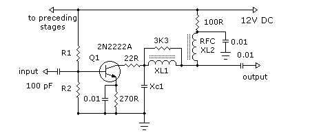
Fig 1.
Let's look at one example of a small signal amplifier, perhaps of the type to follow the previous buffer amplifier. We will assume we are buffering and amplifying our signal from the voltage controlled oscillator tutorial. In those examples we were generating and buffering 1.8 to 2.0 Mhz signals for the 160M band.

Here I've used a pretty standard and cheap transistor for our small signal amplifier. This transistor has some pretty impressive characteristics though.
The configuration is much the same as other class "A" amplifier designs covered in previous tutorials.
The output circuit consists of a low pass filter network which also converts the desired output impedance we want Q1 to see to our standard 50 ohms output.
The 100 ohm resistor, RFC XL2 and the 0.01 uF capacitors are purely for decoupling purposes i.e., to keep RF out of the small signal amplifier power supply as well as other stages. Let's consider firstly the input circuit of our small signal amplifier.
Q1 is biased for DC conditions by R1, R2 and the emitter resistor of 270 ohms in this instance. Alert readers will be aware I like to bias the base voltage of my transistors to about 25% of Vcc (.25 * 12V) or 3V. It follows then that R1 will be about 3 times the value of R2 - think about it!. If the base voltage is around 3V then the emitter voltage is going to be 3v - 0.65V = 2.35V. Don't follow that? Go back to class "A" amplifier designs covered in previous tutorials.
If the emitter voltage is 2.35V approx. then the emitter current Ie through the emitter resistor of 270 ohms must be (from ohms law) 2.35 / 270 = 0.0087 or 8.7 mA. I've also said elsewhere I like base current to be about 1/7th of emitter current - alright these are my foibles and others would disagree. They're welcome to write their own papers.
So base current is going to be about 1 mA and seeing R1 + R2 are connected across 12V it follows that (from ohms law) R1 + R2 = 12V / .001 = 12,000 ohms or 12K. For biasing R1 is 3 times R2 so using simple maths R2 is 25% or 3K and R1 would be 9K which are not necessarily readily available standard values. We will make R2 = 3K3 and R1 = 10K which if you do all your sums is near enough and probably about a third of the values others might use.
So we have our DC conditions satisfied and the 0.01 capacitor in parallel with the emitter resistor means for RF purposes the emitter is at ground potential. This then leaves the output circuit to be discussed. The 22 ohms resistor in the collector circuit is there to discourage parasitic oscillations. RFC XL2 as I said before is only to decouple the power supply and I'd look for a reactance of around 20,000 ohms or at 2 Mhz something like 1 to 2.5 mH.
All this leaves is our low pass filter matching network. First question?? How much output power do we want? Huh? Yep that's how it all works.
Let's say we wanted +17 dBm for a mixer circuit. To the uninformed +17 dBm is a power relationship in milli-watts. Power is always (10 * log of power) so in this case in reverse we divide the 17 by 10 to get 1.7 which is the log of 50 so it follows that +17 dBm is in fact 50 mW of power. Learnt something?
Incidently a power level of 50 mW into 50 ohms also equates to Erms = SQRT ( 0.05 * 50 ) or 1.58V RMS or * 2.828 to get pk-to-pk which is 4.47V PK-PK. Alright how do we design to get 50 mW out of our amplifier? By using the formula R = Vcc2 / (2 * Po) or in our case [ (12V * 12V) / (2 * 0.05) ] = 1440 ohms. Want more power? Change the numbers! Obviously there are limits but you get the idea.
From the above the collector needs to see a load of about 1440 ohms which in turn has to be transformed into our 50 ohm load. By the way, if the amplifier doesn't see a 50 ohm load then all these calculations go right out the window. At the end I show my method of ensuring something like a 50 ohm load and more important the method helps the succeeding stage see a 50 ohm source.
If you have done previous tutorials on filters this is easy. If not then you need to do more work. This is a simple "L" network low pass filter designed in this case to transform 1440 ohms to 50 ohms. Follow these steps where SQRT signifies square-root-of:
1. XL = the SQRT of [(R1 * R2) - (R1 * R1)] = SQRT [(50 * 1440) - (50 * 50)] = SQRT [ 72,000 - 2,500] = SQRT of 69500 = 263.6 ohms
2. Xc = [(R1 * R2) / XL] = 72,000 / 263.6 = 273 ohms
Therefore the reactance of our inductor is about 264 ohms at our frequency of interest and the reactance of our capacitor is about 273 ohms at that same frequency. In the beginning I mentioned a requirement for a 1.8 to 2 Mhz small signal amplifier so we will nominally use 2 Mhz as our cut off frequency i.e. we want to pass all signals below about 2 Mhz but not above (filter out harmonics!).
Here I always see what capacitor has a reactance of 273 ohms at 2 Mhz using the standard capacitive reactance formula Xc = 1 / (2 * pi * Fo * C). Which when algebraically rearranged for our purposes becomes C = 1 / (2 * pi * Fo * Xc ). Slipping 273 ohms for Xc into that formula and 2 Mhz (2,000,000) should get you on your calculator 2.91.. -10 which should then be multiplied by exp 12 to arrive at an answer in pF. Doing that we get an answer of 291 pF which doesn't exist in the real world.
Now you have several choices here. (a) just plonk nearest standard components in for XL and Xc and don't worry about tuning - not recommended. (b) make part of Xc variable e.g. Xc comprises a fixed 270 pF capacitor with a 5 - 50 pF trimmer in parallel or (c) make Xc fixed and XL variable. You can only use the latter option if you have suitable slug tuned inductors available (they ain't cheap but could possibly be salvaged if you know what you are doing).
In the event you chose option (b) the required fixed inductor would be determined from the inductive reactance formula XL = (2 * pi * Fo * L). In ALL examples I use 6.2832 for 2 * pi. For our example we can again rearrange the formula as L = XL / (2 * pi * Fo) and plugging in this case 263.6 ohms XL from above and 2 for 2 Mhz we get L = 263.6 / (6.2832 * 2) = 20.98 uH. That is the inductance you would use, possibly with 60 turns of #26 wire on a T68-2 toroid as only one example.
If you elected method (c) - and this is really cool - I would look back at the capacitor required i.e. 291 pf, use the next lower value which is 270 pF and slot in a variable inductor which will tune through 20.98 uH. Feed a suitable signal to the amplifier, ensure the amplifier is terminated in a suitable fixed 50 ohm load (two 1/2 watt 100 ohm resistor in parallel = 50 ohms) and watch the output on a scope as the slug is adjusted. Wow! In fact you should get a similar effect with the variable capacitor method in (b). Certainly you will then understand why method (a) sucks.
I mentioned earlier how I ensure a 50 ohms load and succeeding stages see a 50 ohms source. I use a 50 ohm 3 dB attenuator. This is a resistive pi network attenuator which consumes 3 dB of power but represents a constant load. You put it in circuit after the last 0.01 uF coupling capacitor after the output.

Now the downside. It consumes power. At - 3 dB that's half the power!!! What the hell just do your sums all over again to produce 100 mW from the amplifier. I would!
In this event your collector load is now 720 ohms, Xc = 197 ohms and XL = 183 ohms. At around 2 Mhz they translate into 403 pF (use 390 pF) and about 14.6 uH.
See - dead easy!
But if you have got this far then send me a courtesy email
NEXT - Power Amplifier Design
the author Ian C. Purdie asserts the moral right to be identified as the author of this web site and all contents herein. All rights reserved. See copying and links. These electronic projects are provided for individual private use and the author assumes no liability whatsoever for the application, use, misuse, of these projects that result in the direct or indirect damage or loss that comes from these projects. All materials are provided for free private and public use. Commercial use prohibited without prior written permission from Ian C. Purdie.
| Revised 6th May, 2000 | My privacy statement | Subscribe to my FREE monthly Newsletter | |
| Email to: Ian C. Purdie | URL: www.integritynet.com.au/~purdic/small-signal-amplifier.htm | Copyright © 1998-1999-2000 by Ian C. Purdie | |