
This site is hosted at WebWizards.Net for better value.
Don't leave this valuable site without visiting my book shop to see my recommendations. This helps keep this site FREE for everyone.
LAST MODIFIED:
Monday, 27-Aug-2001 22:35:07 EDT
YOU ARE HERE: HOME > AMPLIFIERS > BROAD BAND AMPLIFIERS
Broad band amplifiers are amplifiers which will reproduce a wide range of signals without significant loss throughout the pass band. A typical broad band amplifier is a mast head amplifier erected on a TV mast and designed not only to amplify VHF and UHF TV signals but also to establish a low noise figure. Not all broad band amplifiers are that wide so we will consider some examples here.
The first thing I sincerely recommend you do is buy this excellent reference book through my amazon affliate program. Introduction to Radio Frequency Design - Wes Hayward W7ZOI - highly recommended. Paperback and published by ARRL - delivery 3 to 5 weeks. Wes Hayward probably taught me 30% of what I know in electronics - an even better reason.
Why do I personally highly recommend this book? Wes Hayward is the sharpest designer I know and is highly respected as the "guru" and I don't make strong recommendations lightly. At the price ($US 30.00) it is literally the cheapest investment you will ever make in your electronics education - believe me, even if you are not especially interested in radio frequency design you will learn a lot of basic principles which are universal in electronics. And you will write and thank me for doing us both a favour.
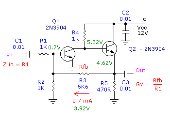
Broad band amplifiers can be designed either with or without broad band transformers. A typical example without broad band transformers is shown in figure 1 below.
Figure 1. - rf buffer amplifier with shunt feedback
Now some very interesting things occur here. Firstly the amplifier is broad band by nature and the bandwidth would be a function of the transistors used. We would not take the expression broad band too literal here. Certainly we would expect several Mhz bandwidth centred around say 20 Mhz. Not exactly a TV mast head amplifier but it would certainly operate quite well at lower frequencies down to audio.
Secondly the input impedance is determined by the resistor R1 while the output impedance initially is probably around R5. Thirdly the voltage gain is determined by the ratio of R3 the feedback resistor Rfb, R3 to R1, the input resistor. In this case 5K6 / 1K or a typical 5.6 voltage gain or 15 dB demanded of any amplifier. If you can't understand the "typical 5.6 voltage gain or 15 dB" then look at decibels for further explanation.
From the Back Cover
This is the handbook for the RF or wireless communications beginner, student, experienced technician or ham radio operator! Although meant for people with a prior foundation in electronics, this book furnishes the reader with valuable information on the fundamental and advanced concepts important to the study and application of RF wireless communications. In this Second Edition of The Complete RF
Technician's Handbook all chapters have been expanded, enhanced and / or
updated....
ORDER NOW! - FROM AMAZON Well how do all these weird things come about in a rf buffer amplifier with shunt feedback? If you have done the basics "small signal transistors" you would know that the base of Q1 must be at 0.7v (although sometimes we use 0.65V - it all depends on which school you went to <G>)
So where can this 0.7V come from? Can't come through R1 because there is a blocking capacitor there ahead of it. How about through R2? Yes, but how? It is supplied by current flowing in R3 a whole 0.7 mA and this by ohms law (again) causes a voltage drop across R3 of 3.92V. The base current of Q1 is sufficiently small as to be ignored.
It follows that the voltage at the emitter of Q2 must be 0.7V + 3.92V = 4.62V and if this is so then the base of Q2 must be that figure plus its base bias of 0.7V or 5.32V and this also happens to be the collector voltage of Q1.
Let's hit this little broad band amplifier with a signal of about 50 mV rms (70mV pk or 140 mV pk-pk) and the input goes from nothing to 70mV then the current flowing in R1 will rise and tend to flow into the base of Q1 and so cause the collector voltage of Q1 to drop. This in turn causes the emitter voltage of Q2 to alter in sympathy and also causes the current flowing in Rfb R3 to similarly decrease.
This process continues so that the base of Q1 remains constantly 0.7V. The effect is that current flowing through R1 supplants current flowing in R3 and this constant 0.7V at the base of Q1 is maintained. Because of this constant value the input base resistance of Q1 is almost zero and the broad band amplifier input resistance is approximated by the input resistor R1 which is "well defined".
Without a whole lot of maths it can be demonstrated that the voltage gain is solely determined by the ratio of R3 to R1 and not by transistor characteristics. Further, significant loads can be placed on the amplifier because whatever the output is, the input always adjusts to 0.7V to follow. Of course there are limits but shunt feedback reduces output impedance. In short, for a few extra components we have an almost "ideal" amplifier.
In the tutorial emitter degeneration we improved performance by splitting the emitter resistor into two resistors and only bypassed one for ac or rf.
Now if you provide feedback in-phase you get an oscillator. What happens in this instance is some of the energy in the output is fed back to add to the input so we have sustained oscillations or a fly wheel effect.
This is most definitely NOT the goal here. We want to do the exact opposite.
We will take some of the output out-of-phase so that it subtracts from the input. This is called negative feedback. It is an enormous aid to stability. This is all toward our goal of a linear amplifier.
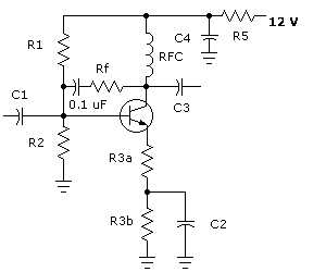
How is this accomplished. Quite easy! Shunt feedback is accomplished by adding one resistor and a capacitor between collector and base of our transistor. Look at Figure 2 below which is simply figure 1 from the emitter degeneration tutorial with that embellishment. For this exercise I'm going to go to an r.f. application and replace resistor R4 with a choke, it could easily be a transformer.
Figure 2. - rf buffer amplifier with shunt feedback and emitter degeneration schematic
Let's look at the choke RFC. What does it achieve for us?. Any inductor resists or opposes a change in current flowingin it. This has the effect of dumping any r.f. voltage through C3 coupling capacitor.
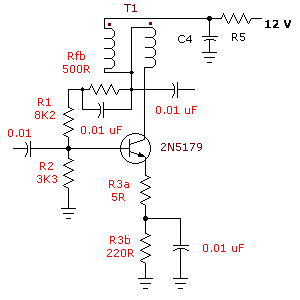
Better still we will replace our RFC with a broadband transformer. In a lot of applications we want a large bandwidth and because our broad band amplifier can be subject to strong in band signals it is necessary to bias our amplifier to a reasonably high standing collector current. We have seen specialised examples where this standing current exceeds 100 mA! In this application we will bias for a modest standing current of 10 mA.
Figure 3. - wideband rf amplifier with shunt feedback and emitter degeneration
If you were paying attention in the tutorial small signal amplifiers you would know I like to bias the base of a transistor at around 25% of Vcc and for a 12V supply this is about 3V and because out Ic is going to be 10 mA we need something around a tenth of that (1 mA) as base current. It follows for 1 mA of base current, the base resistors would total about 12K and in a ratio something like 3K and 9K. Lets make R2 3K3 for the moment and R1 and Rfb combined will total 8K7.
If the base voltage is 3V then the emitter voltage is 2.3V nes pas? With an emitter voltage of 2.3V and a collector current of 10 mA flowing through R3a and R3b they must total
230 ohms.
Now here comes a "neat" trick. If you take the square root of R3a the un-bypassed emitter resistor times Rfb the feedback resistor you arrive at a close approximation to the input imedance! Yes read that again.
So for an input impedance of 50 ohms R3a * Rfb = 2500. Let's look at some standard resistor values. If Rfb were made 510 ohms (or use two 1K resistors in parallel) we need 5 ohms for R3a. If you can't get 5.1 ohms (that's 5R1) use a 4.7 (4R7) ohm resistor. You could use 220 ohms for R3b.
For R2 we used 3K3, make R1 8K2 with of course Rfb being 500 ohms. All that leaves now is the broad band output transformer.
A broad band output transformer of this type is simply wound usually on a ferrite toroid with a reactance equal to 4 to 5 times the nominal primary load impedance at the lowest frequency of interest. In this application our transformer is the 4:1 impedance transfer variety. That means T1 transforms 200 ohms down to 50 ohms. It follows for a reactance of say 800 ohms at 2 Mhz we would need an inductance of about 63 uH.
That could be easily achieved with 30 bifilar turns on an FT-50-61 toroid. Now bifilar simply means take two equal lengths of winding wire, stretch the wires by clamping one end in a vise and pulling gently. Next you have to twist the entire length of the wires until you achieve about one twist per inch. If you have a hand drill bend a nail into a hook shape and tie the other end of the wires to that and clamp into the chuck of the hand drill. While maintaining tension gently twist the wires.
Having twisted the wires you need to wind the turns through the toroid. Looking at figure 3 again note the two brown dots on the transformer. These indicate the two start wires, maybe they were the ends you inserted in the chuck of the hand drill. It is extremely important you observe this polarity or phasing because otherwise it won't work.
Also particularly note the connection from the collector of the transistor to the transformer. It does NOT connect to the output line. All cross connections are denoted by blobs O.K.?
Now any decent broad band amplifier needs a quality transistor. The one indicated a 2N5179 has an Ft of about 1 Ghz. Always select a transistor with an Ft of at least 10 times the highest frequency expected, an Ic rating well inside anticipated currents. Also note some higher current applications often require heatsinking.
Finally the upper frequency limit in you broad band amplifier is often determined by the length of the wire actually used in the transformer. It begins to approach substantial portions of the upper frequency limit's wavelength.
NEW! - How to link directly to this page
Copy and paste the following code for a text link:
and it should appear like this:
This site is hosted at WebWizards.Net for better value.
As you would imagine maintaining this site costs me considerable sums of money in many, many ways. If you believe this site is a valuable and FREE educational resource and, YOU want to keep it that way, then here's how YOU can demonstrate your very practical support for this site..
Thanks to these fine folks making voluntary donations, ensuring this site and our Newsletter remains FREE. Could YOU be listed here for your small contribution in return for your FREE education?. Our grateful thanks.
Please send me your valuable comments and suggestions! Tell your friends, tell a news group, tell your favourite magazine, heck tell the world!
Absolutely essential to keeping abreast of new and updated electronics tutorials is our comments or subscribe to our highly regarded FREE monthly newsletter form. Unsubscribe any time you like. You can view immediate past issues here to see if it is to your liking.
YOU ARE HERE: HOME > AMPLIFIERS > BROAD BAND AMPLIFIERS
the author Ian C. Purdie, VK2TIP of www.electronics-tutorials.com asserts the moral right to
be identified as the author of this web site and all contents herein. Copyright © 2000, all rights reserved. See copying and links.
These electronic tutorials are provided for individual private use and the author assumes no liability whatsoever for the application, use, misuse, of any of these projects or electronics tutorials that may result in the direct or indirect damage or loss that comes from these projects or tutorials. All materials are provided for free private and public use.
Copyright © 2000, all rights reserved. URL - www.electronics-tutorials.com/amplifiers/broad-band-amplifiers.htm
Updated 15th May, 2000
webmaster@electronics-tutorials.com
What are broad band amplifiers?

rf buffer amplifier with shunt feedback

How the rf buffer amplifier works
Broad band rf amplifier using emitter degeneration, shunt feedback
USING OTHER FEEDBACK - shunt feedback combined with emitter degeneration.


Link to this page
Want to create a page link to me from your site? It couldn't be easier. No HTML knowledge required; even the technophobes can do it. All you need to do is copy and paste, the following code. All links are greatly appreciated; I sincerely thank you for your support.
<a href="http://www.electronics-tutorials.com/amplifiers/broad-band-amplifiers.htm" target="_top">visit VK2TIP's Broad Band Amplifiers Page</a>
visit VK2TIP's Broad Band Amplifiers Page
CARE TO BE A PRACTICAL SUPPORTER OF THIS SITE?

Related topics on broad band amplifiers
buffer amplifiers
emitter-degeneration
negative feedback
small signal amplifiers
subscribe to FREE monthly newsletter
join our "electronics discussion group"
Commercial use prohibited without prior written permission from www.electronics-tutorials.com.