most often asked questions about VCO's
Q. What type of VCO's are available from Mini-Circuits?
A.
Mini-Circuits sells fundamental frequency oscillators up to 2GHz and beyond in surface
mount (models JTOS and JCOS), plug in (model POS), and connectorized (model ZOS)
versions.
Q. Generally, how do I select a VCO for a given application?
A.
Narrow band VCO's generally have better phase noise than wide band VCO's. For example,
Mini-Circuits narrow band model JCOS-1100LN exhibits a phase noise of -150dBc/Hz at 1MHz
offset compared to -136dBc/Hz for the wider band model POS-1025 at the same offset
frequency. Application wise, wide tuning VCOb are recommended for electronic counter
measures such as radar, surveillance, etc., and narrow band VCO's are used in phase lock
applications in receiver and transmitter systems.
Q. Can I use Mini-Circuits VCO's with a lower supply voltage?
A.
Yes. Mini-Circuits VCO's can be operated with no damage at a lower voltage however, output
power and tuning range may change. Mini-Circuits offers a variety of specialty oscillators
designed for use with a lower supply voltage. Please consult factory with your specific
requirements.
Q. Is there a delay from the time the supply voltage is applied to the VCO, and the time
when the VCO actually starts to oscillate?
A.
Yes, however the delay time is infinitesimally small. Mini-Circuits VCO's have a very fast
response time to the supply voltage. For Mini-Circuits VCO model POS-535, the switching
delay time is about 130 ns (typ.). Consult factory for further details.
Q. Do Mini-Circuits VCO's oscillate at 0 tuning voltage?
A.
Yes. All Mini-Circuits VCO's are designed to work at a tuning voltage of 0 volts. Some
oscillators may have lower output power at 0 tuning voltage.
Q. When the supply voltage to the VCO changes, what parameters are affected and how?
A.
Both frequency and output power will change. Frequency change is characterized by pushing
and is expressed in MHz per volt change. If the supply voltage is too low compared to the
specified voltage, it may adversely affect the oscillation characteristics, and may even stop
oscillating. If the supply voltage goes too high, power dissipation in the transistors will increase
and will decrease the reliability of the unit.
Q. When the VCO is switched between two control voltages, how long does the
VCO take to move from one frequency to another and settle?
A.
Settling time is a function of the modulation bandwidth. Most Mini-Circuits VCO's exhibit a
modulation bandwidth of greater than 90kHz unless otherwise specified. This corresponds to a
settling time on the order of 0.01 millisecond.
Q. How does the VCO phase noise affect the overall noise of a Phase Locked Loop (PLL)
system?
A.
A conventional PLL is shown in Figure 1, and consists of a VCO phase locked to a stable
frequency reference (refer to Application Note entitled "phase locked loop fundamentals"). The
loop phase detector generates a dc signal to keep the VCO under lock. The reference signal is
usually derived from a crystal controlled oscillator. The phase noise of crystal oscillators are
generally good, but the frequency of oscillation is usually limited to about 200 MHz. In order to
obtain a higher frequency reference, the crystal oscillator output is virtually multiplied. This
multiplication may be done using a phase locked loop as shown. Here, a VCO operating at a
higher frequency is used. It is divided by N for phase locking. With this approach, the reference
frequency is effectively multiplied by N and degrades the phase noise by 20 log N. In spite of
this degradation, the close in noise is good, but the far out noise is worse than that of a free
running oscillator such as a fundamental VCO at the multiplied reference oscillators frequency.
By proper chdce of loop bandwidth of a PLL, the best of the noise of reference and VCO can be
obtained. The loop bandwidth determines the dynamics of the resulting phase locked loop.
Below the loop bandwidth, the noise is essentially the same as that of the multiplied reference.
Above the loop bandwidth, it is essentially the same as that of the free running VCO.
Figure 1
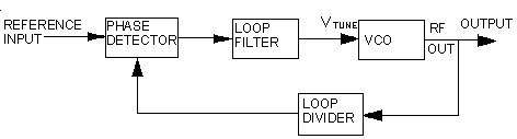
Block diagram of a phase locked loop
Q. Can you explain frequency deviation?
A.
Frequency deviation is how far the center frequency of the oscillator will change as a function
of the control voltage.
Q. What is FM noise or phase noise?
A.
FM noise or phase noise refers to the short term random frequency fluctuations of a signal.
There is a direct relationship between FM noise and phase noise since frequency deviation is
equal to the rate of change of phase deviation (see Application Note entitled "VCO Phase Noise"). Mini-Circuits measures
single sideband phase noise for characterizing short term stability of a signal, since small FM
deviations are difficult to measure.
Q. What is AM noise and how is it caused?
A.
AM refers to the amplitude fluctuations of the signal and is caused by bias current noise
fluctuations and supply voltage variations. The AM component caused by collector current noise
fluctuations may be approximated as follows. For a collector current of Ic, the shot noise
component is 2 qIc where q is the charge on the electron. The percentage of AM due to shot
noise component is therefore: (2(2qIc).100)/ Ic. For 10 mA of collector current, the percentage of
AM is therefore 6.4 x 10⁻¹⁹, which is -182 dBc below the carrier. The AM noise component is
therefore small and can be neglected. The most common source of spurious amplitude
modulation is the DC power supply. A 0.1% change in the resonator voltage corresponds to ± 0.1
% AM on the carrier, which is corresponding to a modulation depth of 0.1/200 = 0.0005. This is
therefore 20 log10 (0.0005) = -66dB below the carrier. Thus, supply voltage noise should be kept
to a minimum.
Q. What is wide band noise floor?
A.
A VCO consists of a tank circuit and a positive feedback amplifier. For offset frequencies
greater than the VCO's half bandwidth, fo/2QL, the phase noise has no positive feedback and is
determined only by the ratio of the oscillator signal level and thermal amplifier noise. If we
assume an 18dB gain for the amplifier, and 6dB for the noise figure of the amplifier, the noise of
the amplifier at its output is given by:
|
No | = | (-174+ 18+6) dBm/Hz |
|
= | -150 dBm/Hz |
Here, -174dBm/Hz represents the input thermal noise power. To minimize the effect of power
supply noise, a low noise power supply should be used. Power supply filtering is discussed in the
Application Note entitled "Reducing Power Supply Noise". For an oscillator generating 10mW of power, the carrier to noise ratio is
given by:
|
C/N | = | 10 - (-150) dBc/Hz |
|
= | 160 dBc/Hz |
Q. How can the VCO influence phase noise in a communication system, such as cellular or
PCN?
A.
A VCO used in a PLL acts as a stable local oscillator. When this is used for down conversion,
the phase noise of the VCO and the incoming RF signal are added together with the thermal
noise of the mixer resulting in the effective noise of the down converted signal. So, to keep the
total noise low, the VCO should have lower phase noise. The noise level that can be tolerated is
dictated by system considerations. For low noise VCO's manufactured by Mini-Circuits, the
noise is typically -150dBc/Hz to -160dBc/Hz, as exhibited in models JCOS-1100LN and
JCOS-1100LN-1 (latter is a non-catalog special! compared to the wide band oscillators, which
are typically l36 dBc/Hz at 1 MHz offset, such as model POS-1025. Mini-Circuits offers a
series of low noise VCO's. Refer to catalog or call for details.
Figure 2
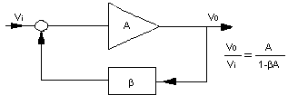
An oscillator may be modeled as the combination of an amplifier and a feedback loop
Figure 3
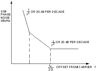
Phase noise characteizationof a VCO
Q. How do I minimize phase noise, and would a narrower range VCO, in general, improve
the noise characteristics of my system?
A.
A VCO may be modeled as a tank circuit and a positive feed back amplifier (Figure 2). The
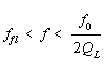
oscillators half bandwidth is fo/2QL where fo is the center frequency
and QL is the loaded Q of the tank circuit. For frequencies within the range
the phase noise will ncrease at 20dB per decade where ffl is the frequency at which 1/f flicker
noise starts to dominate. For frequencies less than ffl, the phase noise will increase by 30dB per
decade. This is illustrated in Figure 3. Close in phase noise is therefore directly related to the Q
of the resonant circuit. High Q or cavity type oscillators provide lower close in noise compared
to low Q VCO's. Also, lower close in noise can be obtained from silicon transistors.
Mini-Circuits uses silicon bipolar transistors for fundamental oscillators. For low noise
applications, narrow band VCO's are recommended. Mini-Circuits has designed very low noise
VCO's using ceramic resonators. They are models JCOS-820WLN, JCOS-820BLN, and
JCOS-1100LN. These VCO's are particularly suitable for applications in wireless products.
Q. What are the benefits of wide band VCO's?
A.
Wide band VCO's can be used in a variety of applications. The following list outlines some of
the benefits of wide band VCO's.
1. In applications such as radar and electronic counter measures, wide band VCO's provide
fast tuning and wide frequency coverage.
2. Fewer VCO's are needed to cover a given frequency range.
3. A standard VCO can be used as a general purpose oscillator for a variety of applications.
This
can result in cost benefits.
4. Some of the wide band applications can be achieved without resorting to switching
VCO's.
5. When frequency pulling is significant enough to shift the VCO outside of its frequency
range,
a wide band VCO can more easily accommodate the correction to the frequency
shift.
Q. What is the best way to specify output power requirements?
A.
Output power is usually measured into a 50 ohm load. Output power requirements should be
specified in dBm, and tolerances in ± dB.
Q. Can you give me an explanation about tuning slope?
A.
This is the slope of the frequency to voltage tuning characteristic at any point and is the same
as modulation sensitivity. The slope could be positive or negative. For a positive slope, the
output frequency increases as the tuning voltage increases. Similarly for a negative slope, the
output frequency decreases as the tuning voltage increases (see Figure 4).
Q. What is monotonic tuning?
A.
A monotonic tuning characteristic means that the frequency is single valued at any tuning
voltage and that the slope has the same sign across the tuning range. All Mini-Circuits VCO's
have a monotonic tuning characteristic and have a positive slope (see Figure 4).
Q. Can you explain tuning linearity and how it is specified?
A.
Tuning sensitivity as a function of tuning voltage is a measure of tuning linearity. For any
given application, specify the minimum and maximum of the tuning sensitivity (see Figure 5).
Q. How does tuning linearity manifest itself in FM/PM transmitters?
A.
In FM/PM transmitters, the information is transmitted by modulating the carrier frequency of
the VCO. A modulating signal at the tuning port modulates the VCO and produces modulation
sidebands. These sidebands can be seen using a spectrum analyzer. In general, a modulating
signal VoSin(fmt) produces sidebands which are 20 log (Vo.K/1.414fm) below the carrier. Here,
K is the VCO modulation sensitivity. If Vo and fm are kept constant, and the VCO frequency is
changed over its range from its low value to its high value, or vice versa, the side band level
relative to the carrier will change. The relative change of the sideband level gives an indication of
how constant K is, which is the modulation sensitivity.
Figure 4
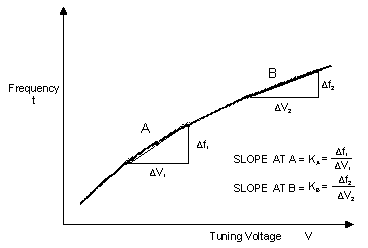
Tuning voltage characteristic of a typical VCO
Q. I notice Mini-Circuits VCO's have lower harmonic content than the competition. What
is your secret?
A.
All octave band VCO's typically have 8 to 10dB second harmonic suppression. This is not
adequate for certain applications. Some Mini-Circuits POS and JTOS models use tracking filters
to increase harmonic suppression to typically 20dB or better. Refer to model data sheets to
determine the oscillators with higher harmonic suppression.
Q. What is the operating temperature range of Mini-Circuits VCO's?
A.
All Mini-Circuits VCO's are designed to operate over the temperature range of -55 C to +85
C.
Q. Are custom VCO's available from Mini-Circuits?
A.
Yes. Custom VCO's engineered with specifications different than standard catalog models are
available from Mini-Circuits. Such requests can best be communicated by sending your requirements to Mini-Circuits applications
department. Our applications engineers stand ready to knowledgeably respond to your custom
VCO requirements.
Q. Are Mini-Circuits VCO's moisture resistant?
A.
POS models are hermetically sealed therefore, no moisture can get in.
Q. What is modulation bandwidth or video bandwidth?
A.
Modulation bandwidth is the modulating frequency at which the frequency deviation
decreases to 0.707 of its dc value. The impedance of the driving source which tunes the VCO is
usually resistive and the VCO's tuning port is mainly capacitave. The combination acts as a low
pass filter. As the modulation frequency increases, the amplitude at the port of this "filter"
reduces. Consequently, the frequency deviation of the VCO reduces. The modulation bandwidth
can be increased by reducing the time constant associated with the tuning port of the VCO. A
high modulation/tuning bandwidth is required for fast tuning VCO's.
Q What is the modulation bandwidth of Mini-Circuits VCO's?
A.
Most Mini-Circuits VCO's are designed to have a 90kHz modulation bandwidth or higher. For
example, in model POS-1060, the modulation bandwidth is 1 MHz typical.
Q. I need to ask questions about VCO's, who can I ask?
A.
Mini-Circuits applications engineers are prepared to respond to VCO questions and
challenges posed by customers, including questions regarding specs, performance, and
applications of our products and your designs. Our enormous database is offered at no extra
charge to eliminate any need for guesswork. Wherever possible, we will courteously recommend
a catalog component or help with a custom solution.
Figure 5
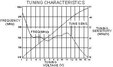 |
V-TUNE |
FREQUENCY
(MHz) |
TUNING
SENSITIVITY |
| 1.0 |
616.50 |
48.0 |
| 2.0 |
656.40 |
39.9 |
| 3.0 |
686.95 |
30.6 |
| 4.0 |
717.23 |
30.3 |
| 5.0 |
748.42 |
31.2 |
| 6.0 |
777.42 |
29.0 |
| 7.0 |
805.13 |
27.7 |
| 8.0 |
835.47 |
30.3 |
| 9.0 |
867.33 |
31.9 |
| 10.0 |
898.35 |
31.0 |
| 11.0 |
932.78 |
34.4 |
| 12.0 |
964.68 |
31.9 |
| 13.0 |
992.13 |
27.5 |
| 14.0 |
1015.10 |
23.0 |
| 15.0 |
1034.03 |
18.9 |
| 16.0 |
1050.93 |
16.9 |