Glossary of VCO terms
VOLTAGE CONTROLLED OSCILLATOR (VCO):
This is an oscillator designed so the output frequency can be changed by applying a voltage to its control port or tuning port.
FREQUENCY TUNING CHARACTERISTIC:
Frequency versus tuning voltage performance for a given VCO. This is usually graphed as
frequency vs. voltage.
FREQUENCY VS. TEMPERATURE
Variation of frequency with temperature at a fixed tuning voltage.
MONOTONIC TUNING:
This refers to the fact that for a given frequency voltage characteristic, the frequency is single
valued at a given voltage, and vice versa. Refer to the applications note entitled "most often asked questions" for further details.
TUNING SENSITIVITY:
This is the slope of the tuning characteristic and is expressed as frequency change per unit
voltage change (MHZ/V, etc.).
TUNING LINEARITY:
The deviation of the frequency versus tuning voltage characteristic from a best-fit straight line.
TUNING NON-LINEARITY:
The extent to which the tuning voltage characteristic falls outside the best fit straight line.
TUNING OR MODULATION, AND DELTA MODULATION SENSITIVITY:
The slope of the tuning voltage characteristic at a given tuning voltage is the tuning or
modulation sensitivity. The difference in modulation sensitivity at two operating tuning voltages
is the delta modulation sensitivity. (For additional information, see the applications notes entitled "most often asked questions").
TUNING SPEED (OR RESPONSE TIME):
This is the time required for the output frequency to settle to within 90 percent of its final value
after applying a step change in frequency. The settling time or tuning speed is related to the
tuning or modulation bandwidth.
VCO INPUT CAPACITANCE:
The total equivalent capacitance seen at the tuning port of the VCO. This parameter is a function
of the amplitude and frequency of the test signal at the tuning port.
MODULATION OR TUNING BANDWIDTH:
The modulating frequency at which the frequency deviation decreases to .707 of its dc value.
This is usually a function of the modulating source impedance, which is typically 50 ohms.
POST TUNING DRIFT:
The application of a step voltage causes the VCO to change its frequency from an initial f1 value
to a final f2 value. The frequency f2 will settle to a stabilized value after some time. Post tuning
drift is the frequency error compared to a final stabilized value at a specified time after the
application of a step voltage. Expressed as frequency error in Hz, kHz, etc. as illustrated in
Figure 1.
Figure 1
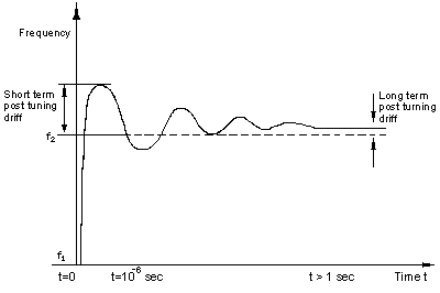
Post tuning drift illustration
FREQUENCY DRIFT WITH TEMPERATURE:
This is the frequency drift of the VCO with temperature at a fixed tuning voltage, and may be
expressed as a relative percentage change per unit temperature, or as a frequency change per unit
temperature.
FREQUENCY PUSHING:
The changing of output frequency corresponding to a given change in the supply voltage at a
fixed tuning voltage (expressed in MHZ per volt).
FREQUENCY PULLING:
Frequency variation caused by changes due to the output load. Usually specified at a load return
loss of 12dB and all possible phases.
OUTPUT POWER:
The fundamental sinusoidal frequency output of the oscillator measured into a 50 ohm load.
OUTPUT POWER VARIATION:
The maximum to minimum power variation (expressed in dB) observed over the specified
frequency range in a 50 ohm system at a given temperature.
OUTPUT POWER FLATNESS:
Variation of the output power from the average output power, expressed in dB.
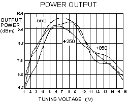
OUTPUT POWER CHANGE WITH TEMPERATURE:
The change in the output power over the temperature range (example using Mini-Circuits Models
POS-765 or JTOS-765 is shown in Figure 2).
Figure 2
HARMONIC CONTENT OR SUPPRESSION:
Harmonics levels are measured relative to the fundamental signal and expressed in dB referenced
to the carrier (dBc).
SPURIOUS RESPONSES OR NON-HARMONIC SPURIOUS CONTENT:
Spurious frequencies are unwanted and non-harmonically related signals present at the oscillator
output. Spurious response is usually expressed in terms of dBc.
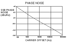
SSB PHASE NOISE:
Single side band phase noise in 1 Hz bandwidth is measured relative to the carrier power at a
given offset from the carrier frequency and is expressed as dBc/Hz, as illustrated in Figure 3
(Mini-Circuits models POS-1025 or JTOS-1025). For more information see the Application Note entitled "VCO phase noise".
FLICKER NOISE:
One of the sources of noise associated with solid state devices, the amplitude of which varies
inversely with frequency. It is also referred to as 1/f noise.
Figure 3
RESIDUAL FM:
This is another form of specifying the frequency stability of a signal source. It is the total rms
frequency deviation frms within a given bandwidth: fa to fb. The bandwidth is usually specified
between 50Hz to 3kHz. Expressed mathematically, we have
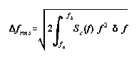
as referred to in the Application Note entitled "VCO phase noise".
Q OR QUALITY FACTOR:
A figure of merit often used in describing the sharpness of a tuned circuit response. A high Q
circuit has a sharper response, and vice versa.
VARACTOR DIODE:
A diode operated in a reverse biased condition providing a junction capacitance that is a function
of the applied reverse bias voltage.
PHASE LOCKED LOOP (PLL):
A feedback circuit in which the VCO frequency and phase is locked to the frequency and phase
of a stable reference signal.
FREQUENCY SYNTHESIZER:
A system that generates any one of equally spaced frequencies within a given band, referenced to
a stable frequency.
PHASE DETECTOR:
A circuit which compares two coherent RF signals and generates a DC output voltage that is a
function of the difference between the phase of two signals.
PHASE DETECTOR GAIN:
This is a constant for a given device, and measured in volts per radian.
BODE PLOT OR BODE DIAGRAM:
A method of describing the transfer characteristic of a circuit or system where the logarithm of
the gain function and phase shift is plotted to a logarithmic base of frequency.
UNITY GAIN:
The gain at which the magnitude of the open loop gain is equal to 1 (or 0 dB).
UNITY GAIN FREQUENCY:
The frequency at which the magnitude of the open loop gain crosses the 0 dB point.
LOOP FILTER:
The loop filter is generally a low pass filter which filters the output of the phase detector and
determines the noise characteristics of the VCO. If the phase detector generates a current output,
then the loop filter will integrate the output signal from the phase detector into a DC voltage to
drive the VCO to a specific frequency. The loop filter may take different forms, such as lag/lead
network, etc.