Super Wide-band RF Choke
Purpose of the Product
Use of Heterojunction Bipolar Transistor technology has resulted in development of super wide-band monolithic microwave amplifiers such as Mini-Circuits ERA series. These amplifiers cover a bandwidth from DC to 8 GHz. They need biasing current injected at the RF output port. As the RF and DC share this port, an inadequately designed DC biasing circuit will degrade the RF performance. It is commonly recommended to use a resistor and RF choke in series with the DC supply. The purpose of the RF choke is to minimize the RF loss caused by the resistor.
Mini-Circuits has developed a super wide-band RF choke covering 50 to 8000 MHz,
which will be available as Model ADCH-80A. This paper will describe the results of using this RF
choke in biasing wide-band amplifier circuits. Performance characteristics such as gain, return
loss, IP3, and power output will be presented and compared against performance measured in a test
fixture, in which biasing current for the amplifier is supplied through the bias-tee which is
internal to the s-parameter test set of the network analyzer.
How a Super Wide-band RF Choke Maximizes Amplifier Performance
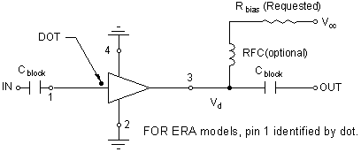
Figure 1 shows the biasing schematic of an ERA amplifier. The biasing
resistor is designated by Rbias. Its value is determined by the device voltage,
the supply voltage, and the desired operating current of the amplifier. For example, for ERA-1
the device voltage is 3.6V. Assuming a supply voltage of 12V, the biasing resistor is given by:
R bias = (V cc - V d)/I d = 210 ohms
where V ccis the supply voltage and I dis the biasing current.
Use of a 210-ohm bias resistor without the RF choke in series will result in 1-dB loss of gain and power
output. If the supply voltage is dropped to 5V, then R bias will be 35 ohms. This will result
in a loss of 3.8 dB in gain and power output, and degradation in return loss. An RF choke in series with
the bias resistor will add an inductive reactance to the shunt impedance, and minimizes the effect of the
resistor on these performance characteristics. This paper presents the performance of the wide-band RF choke,
including the improvement it provides in the wide-band amplifier application.
Fig. 1 Biasing Schematic of ERA amplifier
Description of the RF choke
Commercially available inductors can be used as RF chokes. The low end of the frequency range
of usefulness is decided by the value of the inductance; the higher the value, the lower the frequency. The high
end of the frequency range is determined by the series resonant frequency of the inductor; it tends to decrease
as the value of the inductance increases. Thus, there is clearly a limitation on the bandwidth of usage. Besides
this, inductors are not clearly specified for RF choke applications. This complicates the circuit designer’s job.
Any design changes performed by the inductor manufacturer will have an unknown effect on the circuit.
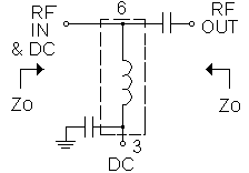
Fig. 2 Photograph of ADCH-80A

Mini Circuits has designed its super wide-band RF choke to optimize performance over a wide band.
Figure 2 is a photograph of the unit and Table-I lists its specifications. It is specified to operate over a frequency
range of 50 to 8000 MHz. This is wide enough to cover the ERA-1 amplifier, specified to 8 GHz. The equivalent inductance
of the RF choke is one microhenry. For comparison, a typical commercially available one microhenry inductor has a series
resonant frequency as low as 90 MHz, which is much lower than that of the RF choke, Model ADCH-80A. Figure 3 shows the
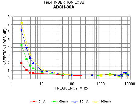
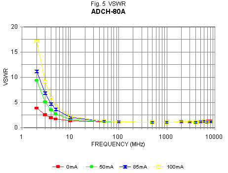
schematic of the circuit used to evaluate the RF choke in a 50-ohm system. Figure 4 plots the insertion loss and Figure
5 the return loss at various currents up to 100 mA. Note the insertion loss and VSWR change very little with change
in current.
Fig. 3 Evaluation circuits
Performance of the RF Choke in Amplifier Applications
To illustrate the use of the RF choke, evaluation boards were built using the ERA-1SM amplifier
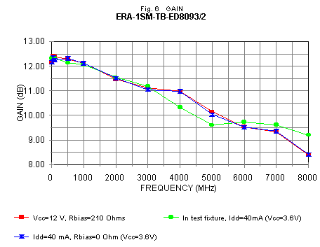
per the schematic in Figure 1. Figure 6 shows the gain of the amplifier with two values of Vcc: 12 V and 3.6 V.
In the first case the biasing resistor is 210 ohms and in the second case it is zero ohms. Note that the gains in both cases
are very close to each other, showing the effectiveness of the RF choke. In practice, a finite biasing resistor dropping a few
volts1 is recommended for bias-current stability unless a constant current source is used for biasing. Also shown in figure 6 is
the gain of the amplifier measured in the test fixture. In this case, biasing current is via the bias tee which is a part of the
s-parameter test set as mentioned above. Note that the gain is very close to that measured in the RF choke evaluation board except
in the range of 7 to 8 GHz. Part of the difference is due to the longer lines which increase the loss of the evaluation board.
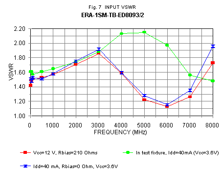
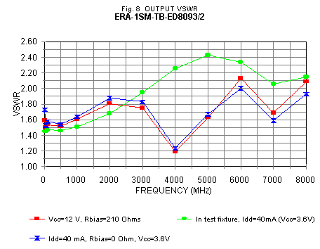
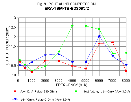
Figures 7 and 8 show the input and output VSWR respectively, for all three cases. The VSWR is again almost same with 210 and zero-ohm biasing resistors. There is slight improvement in the evaluation board; part of the improvement is due to fixed-stub matching. This is required to compensate for the difference in the ground pattern of the evaluation board as compared to the test fixture. Figure 9 shows the compression at 1 dB for the three cases. Another characteristic that can be affected by the RF choke, if its magnetic core is nonlinear, is the third order intermodulation product. Table II shows the IP3 of ERA-1 measured with the fixture and on the evaluation board with the RF choke. No measurable difference was found. Also shown in the table are data on ERA-2 through ERA-6. Note again the closeness of IP3. This demonstrates that the RF choke does not degrade the IP3 of the device.
Table-I: Specification of the RF Choke
| Frequency, MHz | 50-8000 |
| Insertion Loss, dB | 0.4 typ, 1 max |
| VSWR | 1.15:1 typ, 1.35:1 max |
| DC current, mA | 100 max |
| Inductance, microhenries | 7 at 0 mA typ |
| 1.8 at 50 mA | |
| 1 at 100 mA |
Choice of the model depends on the PCB layout (see table below) in the application.
PINOUT CONFIGURATION
| ADCH-80 | ADCH-80A | |
| in | 2 | 6 |
| out | 5 | 3 |
| not used | 1,3,4,6 | 1,2,4,5 |
Table-II: IP3, dBm
| Device | Frequency GHz | In Evaluation board With RF choke |
In Test fixture |
| ERA-1 | 2 | 25 | 25.5 |
| ERA-2 | 2 | 25.5 | 25.6 |
| ERA-3 | 2 | 23 | 23.1 |
| ERA-4 | 1 | 33.2 | 33.2 |
| ERA-5 | 1 | 33.5 | 33.8 |
| ERA-6 | 1 | 37.5 | 37 |
Conclusions
A super wide-band RF choke has been developed for use in biasing wide-band monolithic amplifiers. It can be used in biasing the entire Mini-Circuits ERA series and similar amplifiers operating up to 8 GHz. The choke is tested and specified in a 50-ohm system, to help the circuit designer predict system performance easily.