Biasing ERA Amplifiers
Introduction
The Mini-Circuits ERA series of amplifiers are monolithic devices using gallium arsenide HBT (heterojunction bipolar transistor) technology. The internal circuit configuration is a Darlington pair, embedded in a resistor network. The resistors determine the DC operating point of the transistors, and provide feedback to set RF gain, bandwidth, and input and output impedances to optimum values.
The ERA is a 2-port device: RF input, and combined RF output and bias input, as shown in the schematic diagrams in Figure 1. It has 4 leads including 2 ground leads; connecting both of them to external ground will minimize common path impedance for best RF performance. Multiple transistors are used in ERA-4, -5, and -6 to obtain high output power. This type of circuit is current- rather than voltage-controlled: for a range of current around the recommended value, the device voltage varies much less than in proportion to current. A constant-current DC source would be ideal for providing a stable operating point. By contrast, if a constant voltage DC source were used the current would vary widely with small changes in supply voltage, temperature change, and device-to-device variations. Therefore, use of the constant-voltage mode of operation requires caution.
Figure 1: Schematic Diagrams
| 1a. ERA-1,-2,-3 | 1b. ERA-4, -5, -6 |
 |
 |
A practical biasing configuration is shown in Figure 2. The RF current generated by the ERA in response to an input signal develops an RF output voltage across an external load impedance. Bias current is delivered from a voltage supply Vcc through the resistor Rbias and the RF choke (inductor), shown as RFC in the figure. The resistor reduces the effect of device voltage variation on the bias current by approximating a current source.
Blocking capacitors are needed at the input and output ports. They should be of a type having low ESR (effective series resistance), and should have reactance low enough not to affect insertion loss or VSWR adversely at low frequency. The blocking capacitors must be free of parasitic (parallel) resonance up to the highest operating frequency. Use of a bypass capacitor at the connection to the DC supply is advised to prevent stray coupling to other signal processing components.
Figure 2: Typical biasing Configuration for ERA Amplifiers
- In this circuit, DC blocking capacitors are added at the input port (pin number 1 on the packaged
amplifier) and at the output port (pin 3)
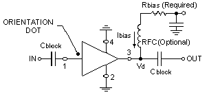
Bias current is given by the equation:
Ibias = (Vcc - Vd) ÷ Rbias
Table 1 lists the values of the bias resistor needed with several values of supply voltage based upon this equation, for each of the ERA models. It also lists the power dissipated by the bias resistor in the 12-volt case, as an example.
Table 1. ERA Bias Resistor Values (in ohms) for Various Supply Voltages
| Model | Bias Current mA | Supply Voltage | Power dissip. in Resistor (mW) for Vcc=12V | ||||
| 5V DC | 9V DC | 12V DC | 15V DC | 20V DC | |||
| ERA-1&SM |
40 |
35 | 135 | 210 | 285 | 410 | 336 |
| ERA-2&SM | 40 | 35 | 135 | 210 | 285 | 410 | 336 |
| ERA-3&SM | 35 | 43 | 157 | 243 | 328 | 471 | 298 |
| ERA-4&SM | 65 | * | 61.5 | 108 | 154 | 230 | 456 |
| ERA-5&SM | 65 | * | 63 | 109 | 155 | 232 | 456 |
| ERA-6&SM | 70 | * | 50 | 93 | 136 | 207 | 456 |
* Not recommended
Advantage of an RF Choke
The advisability of using an RF choke in series with Rbias is evident from the following analysis.
Figure 3 shows an equivalent circuit of the output of an ERA amplifier as a current source in
parallel with an internal 50-ohm source resistance, loaded by both Rbias and an external 50-ohm
load. The current in the 50-ohm load is:Isource x Rbias ÷ (2 Rbias + 50)
and the loss in power gain relative to not having the output loaded by Rbiasis:
20 log [(2 R>bias + 50) ÷ 2 Rbias] dB.
Figure 3: Effect of Bias Resistor on the Output, Without an RF Choke
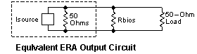
Suppose, for example, that model ERA-4 is used with a 12-volt supply without a choke. From the above expression, the effect of the 108-ohm bias resistor (from Table 1) is found to be a 1.8 dB reduction in the gain of the amplifier.
An RF choke should be chosen such that its reactance is at least 500 ohms (10 times the load impedance) at the lowest operating frequency. It must also be free of parasitic (series) resonance up to the highest operating frequency.
Effect of Bias Resistor Value
Increasing the resistor value reduces the variation in bias current making RF performance, especially the 1-dB compression point, more constant. The device voltage Vd is a function of both Ibias and temperature T.
Typical voltage at several values of current is given in Table 2; the variation is expressed in the
right-hand column as the rate of change,  Vd / Ibias, in mV per mA. (The recommended
operating points are shown in bold type.)
Vd / Ibias, in mV per mA. (The recommended
operating points are shown in bold type.)
Device voltage decreases with increasing temperature as shown in Table 3; the average rate of
change is Vd / T, in millivolts per degree C.
Table 2 ERA Device Voltage vs. Current
| Model No. | Bias Current, mA |
Typ. Device Voltage, volts |
Typ. Device Voltage Variation with
Current, Vd/
Ibias (mV/mA) |
| ERA-1, -2 & SM |
35 | 3.5 | 20 |
| 40 | 3.6 | ||
| 45 | 3.7 | ||
| 50 | 3.8 | ||
| ERA-3 & SM |
30 | 3.5 | 10 |
| 35 | 3.5 | ||
| 40 | 3.6 | ||
| ERA-4 & SM |
55 | 4.9 | 8 |
| 65 | 5.0 | ||
| 70 | 5.0 | ||
| 80 | 5.1 | ||
| ERA-5 & SM |
55 | 4.8 | 8 |
| 65 | 4.9 | ||
| 70 | 4.9 | ||
| 80 | 5.0 | ||
| ERA-6 & SM |
55 | 5.2 | 20 |
| 70 | 5.5 | ||
| 75 | 5.6 | ||
| 80 | 5.7 |
Table 3 ERA Device Voltage vs. Temperature
| Model | Device Current mA |
Device Voltage, volts @ Temperature | Typical Sensitivity of Device Voltage to Temperature Vd/T
(mV/°C) | |||
| -45°C | -25°C | +25°C | +85°C | |||
| ERA-1 & SM | 40 | 3.77 | 3.75 | 3.60 | 3.47 | - 2.5 |
| ERA-2 & SM | 40 | 3.75 | 3.72 | 3.60 | 3.49 | - 2.1 |
| ERA-3 & SM | 35 | 3.64 | 3.54 | 3.49 | 3.37 | - 2.0 |
| ERA-4 & SM | 65 | 5.31 | 5.20 | 5.05 | 4.85 | - 3.2 |
| ERA-5 & SM | 65 | 5.15 | 5.05 | 4.92 | 4.71 | - 3.1 |
| ERA-6 & SM | 70 | 5.76 | 5.74 | 5.60 | 5.42 | - 2.9 |
Based upon the above definitions for device-voltage variation, the variation of current with temperature can be derived:
Ibias = [Vcc - Vd(Ibias, T)] ÷ Rbias'
where Vd(Ibias', T) = V0 + (Vd/Ibias)
·Ibias + (Vd/T)·(T - T0)
The "" ratios are the coefficients from Tables 2 and 3, and V0 and T0 are constants. Combining
terms and solving for Ibias:
Ibias = [Vcc - (Vbias + (Vd/Ibias)]
Differentiating with respect to T:
Ibias/T = -(Vd/T)
÷ [Rbias + (Vd/Ibias)]
To illustrate the effect of supply voltage, let us consider two examples for ERA-1, based upon Tables 1, 2, and 3. For Vcc = 5 volts and Rbias = 35 ohms,
Ibias/T = - (-2.0) ÷ (35 + 20) = .036 mA/°C.
Over an operating temperature range of -45 to 85 degrees C, the total variation in current for this example will be 4.7 mA, which is more than 10% of the recommended value of current. The consequence is about 3.5 dB variation in output power at 1-dB compression.
For the second example, try Vcc = 12 volts and Rbias = 210 ohms. A similar calculation yields 1.06 mA total variation in current, which causes only ¼ as much effect on RF performance.
Minimizing Power Dissipation
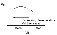
In addition to bias current stability, stability of power dissipation of the ERA device is favored by using a high Vcc value. This is because of the negative temperature coefficient of device voltage Vd. In particular, if Vcc is at least 2 times Vd, then PD, the ERA power dissipation decreases with increasing temperature, as shown by the following analysis:
PD = Vd·Ibias = Vd (Vcc - Vd) ÷ Rbias
Taking the derivative of PD with respect to Vd and setting it equal to zero, we find that the maximum value of PD occurs when Vd = Vcc ÷ 2. This is illustrated in Figure 4.
Figure 4: Variation of ERA Power Dissipation with Temperature, for Device Voltage Above, and Below, Half the Supply Voltage Value
Let us see what happens to power dissipation in the case of ERA-5 between 25 and 85 degrees C, for two values of supply voltage: one less than, and another greater than, twice the value of Vd. We will use 65 mA and 4.9 V as the nominal (room temperature) values of Ibias and Vd.
For Vcc = 5.5 V, Rbias = 9.2 ohms. Using the value -3.1 mV/°C for the Vd temperature coefficient from Table 3 and the above equation, PD increases from .320 watt at 25°C to .403 watt at 85°C. Considering the thermal resistance of ERA-5 (junction-to-case) of 278°C/W, this increase in power dissipation results in 23°C higher junction temperature than if dissipation were constant. The consequence in reliability is almost a decade reduction in MTTF.
Now, try Vcc = 12 V, for which Rbias = 109.2 ohms. For this case, PD decreases from .319 watt at 25°C to .315 watt at 85°C.
Optimum Bias Current
Within the range of bias current listed in Table 2 for each ERA model, a value can be chosen to adjust gain and output power as needed. Recommended values are shown in bold type, and represent operating conditions for which junction temperature and reliability (MTTF) have been established. Higher currents than those listed could cause excessive junction temperature and premature failure. Substantially lower currents, while not degrading device reliability, could cause unpredictable RF performance because of non-optimum internal operating points.
Temperature Compensated Bias Network
An alternative method of biasing the ERA which allows use of lower supply voltage while maintaining bias current stability and reducing power dissipation in the bias resistor is to use a temperature compensating bias network in place of the single resistor Rbias. The network consists of a linear positive-temperature-coefficient chip thermistor such as KOA type LT73, in parallel with a regular chip resistor, and should be designed so that its resistance increases with temperature just enough to make up for the decrease in device voltage, causing the ERA current to remain constant.
Commercially available chip thermistors such as the type noted above have a very high TCR ( temperature coefficient of resistance), +4500 ppm/°C, for resistance values in the range useful for the ERA bias network, 51 - 510 ohms. The temperature coefficient needed for Rbias is much less than this, and thus achievable by using the 2-components (resistor and thermistor) in parallel.
We now derive the values of the network components. Let R be the resistance of the regular resistor, and Rt the 25°C resistance of the thermistor.
Let kb be the fractional increase in Rbias needed at the maximum operating temperature relative to 25°C: (hot resistance - 25°C resistance) ÷ 25°C resistance.
Let kt be the fractional increase in resistance of the thermistor, (4500 x10-6) x (maximum operating temperature - 25°C).
Because the resistor and thermistor are in parallel they must satisfy:
Rbias = R·Rt ÷ (R + Rt) at 25°C, and
(1 + kb)Rbias = R·Rt(1 + kt) ÷ [R + Rt(1 + kt)] at the maximum operating temperature.
Solving these equations yields:
R = Rbias·kt(1 + kb) ÷ (kt - kb), and Rt = Rbias· kt(1 + kb) ÷ [kb (1 + kt)]
Let us compare simple resistor biasing with the temperature compensating network for biasing an ERA-6 with a 7.0 V supply. Let Ibias = 70 mA and Vd = 5.60 V(at 25°C), using the values from Table 3. Therefore, Rbias = 20.0 ohms. At 85°C, Vd is 5.42 V. If we use an ordinary resistor for Rbias without a thermistor, the current will increase to 79 mA.
Now, we compute the network component values needed to make the current 70 mA at 85°C as well as at 25°C. At 85°C, given that Vd = 5.42 V, Rbias must become 22.57 ohms; thus kb= (22.57 - 20.0) ÷ 20.0 = .1285. Also, kt = (4500 x10-6) x (85° - 25°) = .27. Applying the formulas,
R = 20.0 x .27 (1 + .1285) ÷ (.27 - .1285) = 43.1 ohms
Rt = 20.0 x .27 (1 + .1285) ÷ [.1285 (1 + .27)] = 37.3 ohms
If the thermistors are available only in "5% values", sufficiently close compensation is obtained by using Rt = 36 ohms and R = 45 ohms (for 20-ohm parallel equivalent).
For different supply voltages and device operating points different resistor and thermistor values are needed, but the same concept and method can be used. The benefit is the ability to keep the device current constant over temperature, thereby avoiding increase in power dissipated in the amplifier and reduction in MTTF.
We have not mentioned the resistance-temperature coefficient of the ordinary resistor in the bias network. The reason is that thick film chip resistors typically have a coefficients of ±100 ppm/°C. This is about 2% of the TCR of the thermistor, and does not influence the results significantly. A word of caution is due regarding the thermistor, however. Its temperature characteristic is controlled only at 25°C and at 75°C. The user should test actual circuit operation at other temperatures of interest.