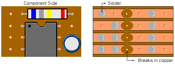
When I first started with electronics I began soldering components on stripboard. Most of you probably know it, among other names, as Matrixboard, Veroboard, Perfboard, etc. You may recognize it as a board having (usually) 1-tenth-inch spaced, pre-drilled holes and copper strips attached to the rear of the board (see below).
This is still ideal for making prototype circuits but it does have obvious limitations. Nowadays I design all my circuit schematics and PCB artwork using nothing other than the Micro$oft Paint program included with Windoze! - "How?", I hear you ask - "Easy!", say I - Just read on for a detailed description...
First, you must have the following four files on your hard drive:
To do this simply place your cursor over each image in turn (below) and right-click with the mouse.
In the following pop-up menu, select 'Save Picture As...' then choose 'BMP' format and your chosen directory.
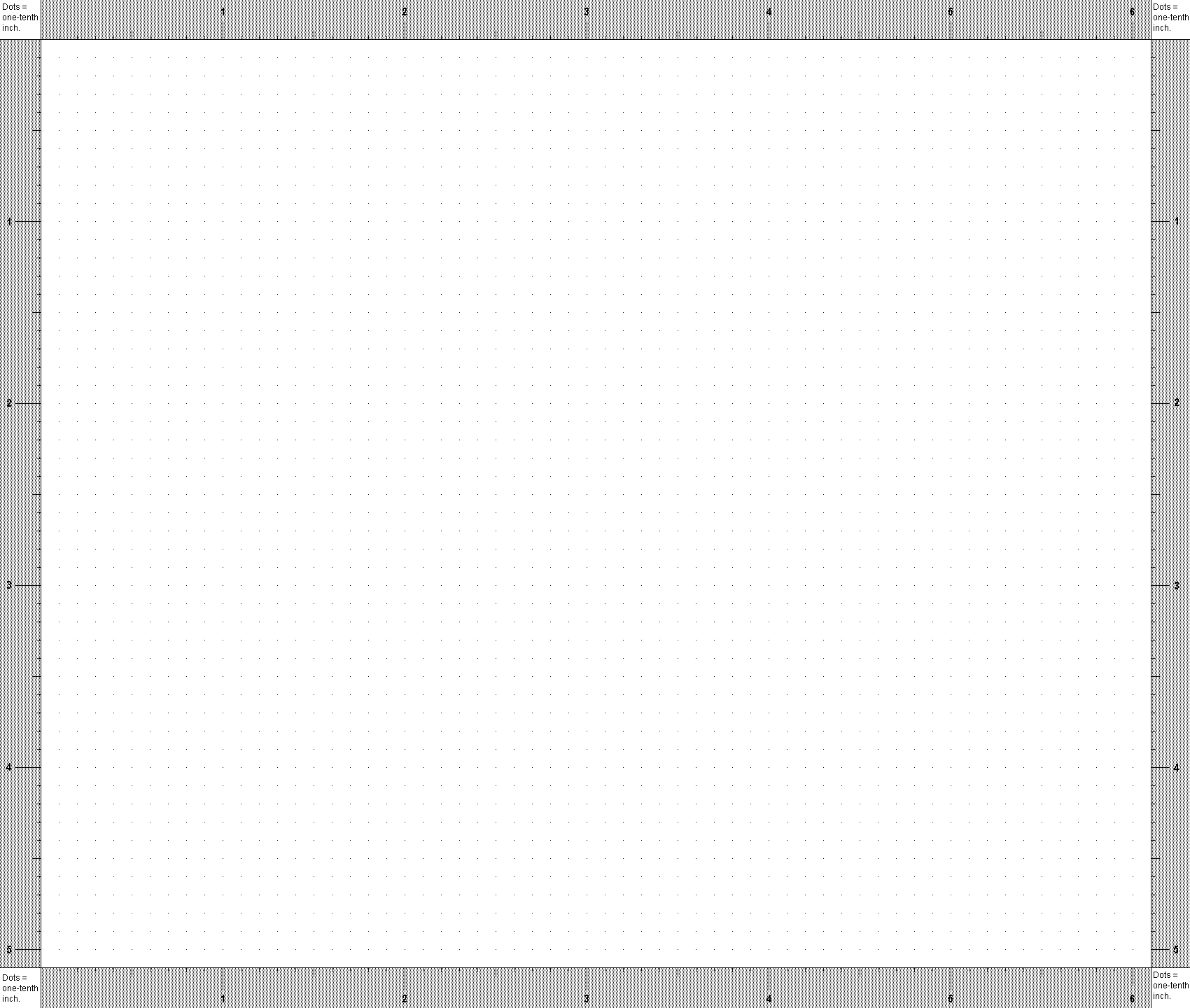
eg: C:\PCB\Grid.bmp.
OK - Now you have all the necessary files to draw your own schematics and PCB's.
Let's begin...
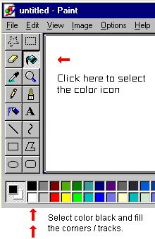
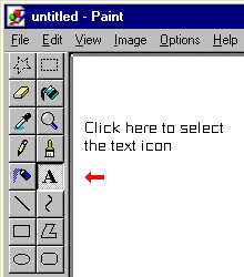
| We need to have two (2) instances of MS Paint running. For copy/paste to work, we have to select, in both instances, these icons (shown with arrows). | 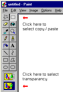
|
|---|
| Have the Color Palette on view (CTRL+A). Set the attributes to 2-color black & white (CTRL+E) Left-click the color Black; right-click the color White. NOTE: For clarity purposes, the Palette shown here has the attributes set to 'Color'.
| |
|---|
To see an example, we'll design a pcb for a simple pre-amplifier one stage at a time.
STEP 1
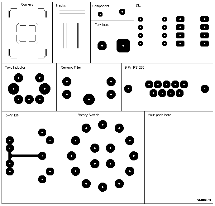
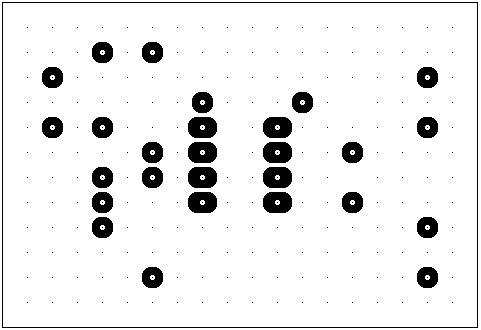
| First copy/paste all your pads to the grid template, remembering at this stage to draw your design as though looking from the component side.
| 
|
|---|
STEP 2
After the pads we add the | tracks and corners... |
|---|
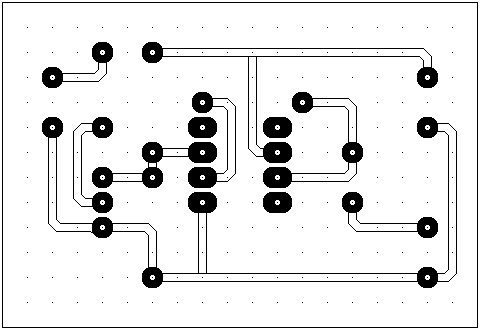
STEP 3
| ...now color all the tracks black...
| 
Note how I've dotted-in where the verticle tracks meets the horizontals - this gives a more neater finish.
| | |||
|---|---|---|---|---|---|
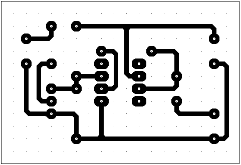
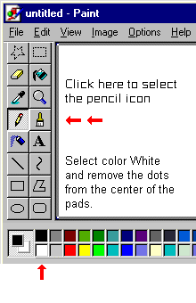
STEP 4
|
Finally, remove the unwanted dots with the tool icons shown below. | A good tip is to use CTRL+PG UP / CTRL+PG DN for zooming in / out of a particular area. 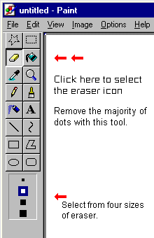
| ||
|---|---|---|---|
STEP 5
| At this stage I usually add some text to the artwork. This makes it easier to define which way to place the artwork on the copper board before the etching process - we don't want a mirror image of what the design should be!
| 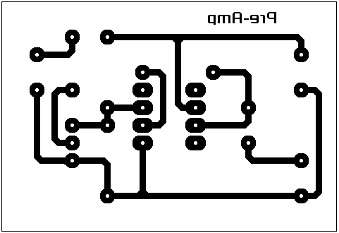
The final artwork without any dots. Remember to reverse any text before printing.
| | |||
|---|---|---|---|---|---|
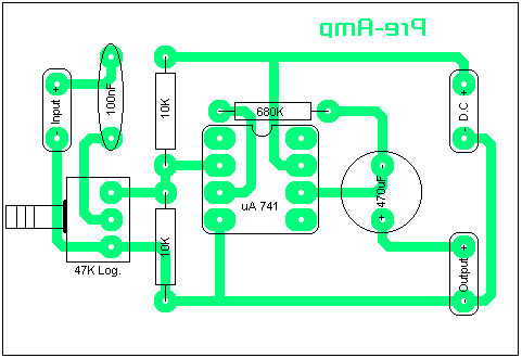
STEP 6
| Finally, the following picture is with the attributes changed to 'Color' (remember to save with a different file name!). Fill in the pads and tracks with a bright color from the Color Palette to give a 'see-thru' appearance then populate the board with the components from the Overlay bitmap. Of course, you don't need do this but if you intend putting your designs on your Webpages it helps readers to see where each component will be.
| 
|
|---|
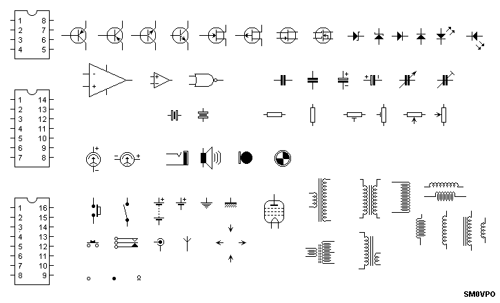
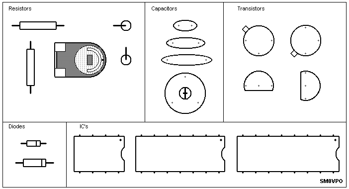
All my schematic diagrams are also drawn using the same copy / paste method. This time copy from the Symbols bitmap file and paste to the Grid template. As you get more confident with the way things work you'll probably find it better to paste to a new black & white file. - ie: not the Grid file.
For straight lines between connections simply click the Line icon - this has five different levels of thickness. I use the thinnest 1-pixel option for normal line connections and the middle option 3-pixel for ground rail connections.
Incidentally, If there's any components you don't see on the Symbols or Overlay bitmaps then simply draw your own with M$Paint... Have fun!
![]()
Best Regards... Pete
http://www.keirle.fsnet.co.uk