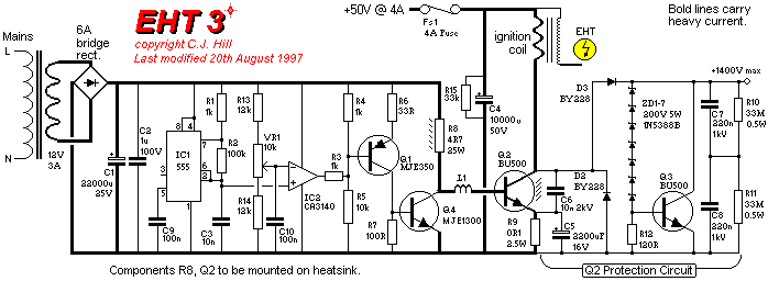
The EHT3 project uses a 555 timer IC to generate a 720Hz triangle waveform (at pin 2 of the IC). This waveform is of about 50% duty cycle. This triangle waveform is compared to a fixed voltage with a comparator, IC2. The fixed voltage can be varied by potentiometer VR1. The output of the comparator is a 720Hz square wave of variable duty cycle. The potentiometer must be adjusted so that Q2 is near to 0% duty cycle (ie it spends the majority of the time off).
The square wave is used to drive the final switching transistor Q2 via intermediate transistors Q1 and Q4. The switching transistor Q2 is a BU500 which is capable of withstanding 1500V at its collector when its base and emitter are grounded. The BU500 switching transistor, Q2, has a protection circuit connected accross its collector and emitter which does not allow the voltage to rise above 1400V. This protection circuit is based on zener diodes ZD1 to ZD7 and another BU500 transistor, Q3. When Q2 switches off the voltage at its collector rapidly rises. At some point the voltage becomes large enough for D2, a BY228 diode, to conduct. The capacitors C7 and C8 charge up. When the voltage on these capacitors becomes larger than 1400V, ZD1 to ZD7 start to conduct. ZD1 to ZD7 are only rated to dissipate 5W each, and I have found by experience with earlier versions that this is not enough (I've blown quite a few zeners). So some of the current that flows through ZD1 to ZD7 is routed to Q3 base. This transistor then takes some of the load. Note that I have in the past even overloaded this transistor. If this causes a problem a resistor (example 100W mains light bulb!) can be put in the collector lead. Another problem can be that ZD1 to ZD7 'leak' a small current even though they have not reached their zener voltage. This current is usually very small, so when it flows through R12 the voltage at the base of Q3 is insufficient for it to turn on. Without R12 this would not be the case as the current would flow through Q3 base hence turning it on.
So ZD1 to ZD7 and Q3 have the effect of clamping the voltage at Q2 collector to 1400V max. Q2 collector is rated to 1500V so there is 100V safety margin.
D2 is used to prevent the collector of Q2 swinging to large negative voltages as the primary of the ignition coil 'rings'.
The DC resistance of the secondary of the ignition coil I am currently using is 7k. The resistance of the connecting leads that I was using was 17k. These leads were of the type commonly used in cars as spark plug leads. They are made of a carbon based conductor. So with a DC current 2.43 times as much heat would be dissipated in the connecting lead as in the transformer winding! I now use copper wire for the connecting lead, and my EHTA design will have a much lower secondary resistance.
If you would like to see data sheets of some of the components used for EHT3, you need Adobe's Acrobat program: