Switch Mode Power Supplies are the current state of the art in high efficiency power supplies. Conventional series-regulated linear power supplies maintain a constant voltage by varying their resistance to cope with input voltage changes or load current demand changes. The linear regulator can, therefore, tend to be very inefficient. The switch mode power supply, however, uses a high frequency switch (in practice a transistor) with varying duty cycle to maintain the output voltage. The output voltage variations caused by the switching are filtered out by an LC filter.
SMPSs can be used to step-down a supply voltage, just as linear supplies do. Unlike a linear regulator, however, an SMPS can also provide a step-up function and an inverted output function. Typical applications are given below.
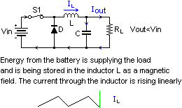
Typical application for a ste-down switching regulator:
Generation of 5V for TTL-based circuits from a 12V battery (particularly suitable if the 12V battery has limited capacity, as switching regulators are far more efficient than linear regulators).
Typical application for a step-up switching regulator:
Generation of 25V from a 5V supply in an EPROM programmer.
Typical application for an inverting switching regulator:
Generation of a double-ended supply from a single-ended for OP-AMP.
Generation of a negative bias for MOS devices eg Dynamic RAMS.
The term switch mode regulator is used to describe a circuit which takes a DC input and provides a DC output of the same or opposite polarity, and of a lower or higher voltage. Switch Mode regulators use an inductor and there is no input to output regulation.
The term switch mode converter is used to describe a circuit which takes a DC input and provides a single or multiple DC outputs, again of same or opposite polarity and lower or higher voltage. Converters use a transformer and may provide input to output isolation.
The term Switch Mode Power Supply or SMPS is used to describe switch mode regulators and converters.
When discussing SMPS circuits, the different topologies are often referred to as 'Forward' or 'Flyback'
A Feed Forward SMPS circuit will supply energy to the output capacitor when the switching element (transistor) is switched on.
A Flyback SMPS circuit transfers energy (from an inductor) to the output capacitor when the switching element (transistor) is switched off.
The current-boosted buck converter uses a transformer to increase output current above the maximum current rating of the switch (which is a transistor in a practical circuit). The current-boosted circuit does so at the expense of increased switch voltage during switch-off time. The increase in maximum output current over a standard buck converter is equal to input voltage divided by output voltage, plus turns ratio times the input-output differential. For example, in a 15V to 5V current-boosted buck converter, with a 1:4 turns ratio, the increase in output current is double: 15/(5+1/4x15-5), or 2. This is a 100% increase in output current. However, the maximum switch voltage for a current-boost buck is increased from input voltage to input voltage plus output voltage divided by the turns ratio. Using the 15V to 5V converter, the maximum switch voltage is 15+5/turns ratio, or 15+5/0.25=35.

In a forward (or buck) regulator power is continuously supplied to the outlet\filter capacitor. In a boost regulator, however, energy is pumped in a cyclic manner. The filter capacitor therefore has to be of a higher value.
The boost regulator, like the flyback regulator, pumps energy into the outlet\filter capacitor in a cyclic manner, and it is therefore desirable to operate in the discontinuous mode with a fixed peak current through the inductor.
The diode conduction time in a boost regulator, unlike the flyback regulator, is not fixed, but varies with the input voltage.
Ipk = 2 x Iout,max x (Vout / Vin,min)Output voltage is regulated by controlling the duty cycle.
Vout = ((Ton / Tdon) + 1) x VinRipple voltage is directly proportional to diode conduction time.
Tdon max = (L x Ipk) / (Vout - Vin,max)
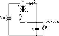
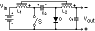
The flyback regulator circuit shown below can be used as a step-up or step-down circuit.
 |
 |
In a forward (or buck) regulator power is continuously supplied to the outlet\filter capacitor. In a flyback regulator, however, energy is pumped in a cyclic manner. The filter capacitor therefore has to be of a higher value.
Flyback regulators can operate in one of two modes: Continuous or Discontinuous. In Continuous mode, a large value of inductor is used such that the current in the inductor never falls to zero. In Discontinous mode, the current in the inductor falls to zero before the switch closes. Usually the circuit is designed such that at worst case conditions (max output current, min input voltage) the current only falls to zero for an instant, ie as soon as the diode stops conducting the switch is closed.
For a flyback regulator, the peak current is given by:
Ipk = (Vin x Ton)/L
where:The conduction time of the diode (which may or may not be the same as the off time of the switch) is given by:
Tdon = (Ipk x L) / Vout
where:The output power from a flyback regulator is given by:
Pout = Vout x Iout = 0.5 x L x Ipk^2 x f
where:Iout is also the average current through the diode (since all output current must flow through D:
Iout = (Ipk / 2) x (Tdon x f)
where:The reverse polarity output voltage is given by:
Vout = (Pout x Rl)^0.5
or:
Vout = Ipk x ((L x f x Rl)/2)^0.5
where:
Vout = Average output voltage - Volts
Pout = Average Output power - Watts
Rl = Load Resistance - Ohms
Ipk = Peak current - Amps
L = Inductance - Henries
f = Frequency of operation - Hertz
The output voltage of the circuit can be regulated by operating the circuit at a fixed frequency and varying the transistor duty cycle. However, because of the pumping action, the output voltage sags while the transistor switch is on and rises when the transistor is off. This makes the circuit difficult to control in a fixed frequency manner. A better approach to controlling the flyback converter when operating in the discontinuous mode is to have a fixed peak current in the inductor and hence fixed anode conduction time. The transistor switch 'on' time can then be varied inversely to any changes in the output voltage. This gives rise to the circuit having variable frequency of operation.
In 1978, the US Patent Office granted Dr Slobodan Cúuk of CalTech (pronounced Chook) a patent for the design of a new SMPS topology. The benefits of his new topology include increased efficiency, low input and output current ripple, minimal RFI and small size and weight.
The series of diagrams below shows how the Cúuk circuit is derived.
Firstly, consider a boost converter followed by a buck converter:
![]()
If the diodes are thought of as switches, then the two switch-and diode sets could be replaced with a DPDT switch:
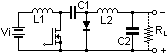
The DPDT switch and shunt capacitor can be replaced with an SPST switch and series capacitor, providing that a reverse of output polarity is accepted:
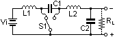
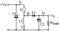
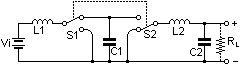
The circuit is an example of a Cúuk SMPS. A practical realisation could be as follows:
The DC voltage transformation ratio M is M=D/D', where D is the duty ratio (fractional on-time) of the transistor switch operated at a switching frequency 1/Ts, and D'=1-D is the complementary duty ratio (fractional offtime). For a DC input voltage Vi, the output voltage is Vo=MVi. The converter thus has a step down ratio for D<0.5 and a step-up ratio for D>0.5. The other principal feature is that both the input and output currents are non-pulsating, both being smoothed by the input and output inductors. These inductors also eliminate current surges in the transistor switch at power-on and power-off, which is often a difficult problem to solve.
Theoretically, the output capacitance C2 is not needed, but is usually included to absorb the load current fluctuations. The Cúuk converter is unique because energy transfers capacitively from the input to the output, instead of inductively as in all previous converters.
A capacitor of 1uF charged to 50V has a stored energy of 1.25mJ, equal to an inductor of 2.5mH passing 1A. The size of a 1uF 50V capacitor, however, is considerably smaller than a 2.5mH 1A choke. Therefore capacitive energy transfer is more effective on a per unit size or weight basis than inductive energy transfer.
Because the input and output inductor currents are essentially constant, the switching current is confined entirely within the converter in the transistor-coupling capacitor-diode loop. With careful layout, this loop can be made physically small, which will reduce the radiated RFI from the magnetic field. In addition, the voltage and current waveforms in this converter are particularly clean, with very little ringing or overshoot; very little snubbing is needed.
Cúuk References
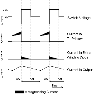
The 'extra' winding of a forward converter's transformer ensures that at the start of a switch conduction, the net magnetisation of the transformer core is zero. If there were no extra winding, then after a few cycles the transformer core would magnetically saturate, causing the primary current to rise excesively, so destroying the switch (ie transistor).
The diode on the secondary that is connected between the 0V line and the junction of the inductor and rectifiying diode is often called the 'flywheel diode'.
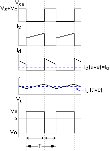
Waveforms for the forward converter are shown below
The output voltage of a forward converter is equal to the average of the waveform applied to the LC filter and is given by:
Vout = Vin x (n2/n1) x (Ton x f)
where: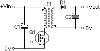
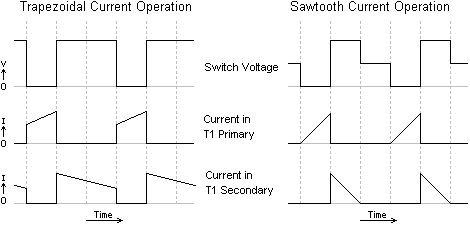
The output voltage for a flyback converter (trapezoidal current flow operation) may be calculated as follows:
Vout=Vin x (n2/n1) x (Ton x f) x (1/(1-(Ton x f)))
where:The control circuit monitors Vout and controls the duty cycle of the drive waveform to Q1.
If Vin increases, the control circuit will reduce the duty cycle accordingly, so as to maintain a constant output. Likewise if the load is reduced and Vout rises, the control circuit will act in the same way. Conversely a decrease in Vin or increase in load, will cause the duty cycle to be increased.
It can be seen that the output voltage changes when the duty cycle, Ton x f, is changed. However the relationship between the output voltage and duty cycle is not linear, as was the case with the forward converter, but instead it is a hyperbolic function.
The current flow in a flybcak converter can have either trapezoidal or sawtooth characteristics, as seen below. The trapezoidal current characteristic is due to the switching transistor turning on again before the secondary current has dropped to zero. Whilst the sawtooth characteristic is due to the secondary current falling to zero and there being a period of 'dead time' when there is no current flow in either secondary or primary.
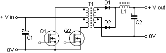
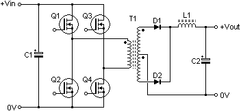
The push pull converter belongs to the feed forward converter family. With reference to the diagram above, when Q1 switches on, current flows through the 'upper' half of T1's primary and the magnetic field in T1 expands. The expanding magnetic field in T1 induces a voltage across T1 secondary, the polarity is such that D2 is forward biased and D1 reverse biased. D2 conducts and charges the output capacitor C2 via L1. L1 and C2 form an LC filter network. When Q1 turns off, the magnetic field in T1 collapses, and after a period of dead time (dependent on the duty cycle of the PWM drive signal), Q2 conducts, current flows through the 'lower' half of T1's primary and the magnetic field in T1 expands. Now the direction of the magnetic flux is opposite to that produced when Q1 conducted. The expanding magnetic field induces a voltage across T1 secondary, the polarity is such that D1 is forward biased and D2 reverse biased. D1 conducts and charges the output capacitor C2 via L1. After a period of dead time, Q1 conducts and the cycle repeats.
There are two important considerations with the push pull converter:
These criteria must be satisfied by the control and drive circuit and the transformer.
The output voltage Vout equals the average of the waveform applied to the LC filter:
Vout = Vin x (n2/n1) x f x (Ton,q1 + Ton,q2)
where:The control circuit monitors Vout and controls the duty cycle of the drive waveforms to Q1 and Q2.
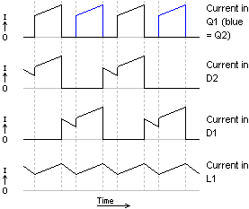
If Vin increases, the control circuit will reduce the duty cycle accordingly, so as to maintain a constant output. Likewise if the load is reduced and Vout rises the control circuit will act in the same way. Conversely, a decrease in Vin or increase in load, will cause the duty cycle to be increased. The diagram below shows associated waveforms from the push pull converter.
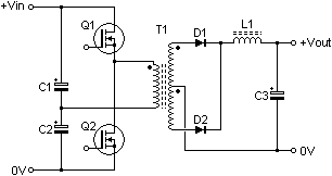
The half bridge converter is similar to the push pull converter, but a centre tapped primary is not required. The reversal of the magnetic field is achieved by reversing the direction of the primary winding current flow. This type of converter is found in high power applications.
For the half bridge converter, the output voltage Vout equals the average of the waveform applied to the LC filter
Vout = (Vin/2) x (n2/n1) x f x (Ton,q1 + Ton,q2)
whereNote that Ton,q1 = Ton,q2 and that Q1 and Q2 are never conducting at the same time.
The control circuit of a half bridge converter is similar to that of a push-pull converter
The full bridge converter is similar to the push pull converter, but a centre tapped primary is not required. The reversal of the magnetic field is achieved by reversing the direction of the primary winding current flow. This type of converter is found in high power applications.
For the full bridge converter, the output voltage Vout equals the average of the waveform applied to the LC filter
Vout = Vin x (n2/n1) x f x (Ton,q1 + Ton,q2)
whereDiagonal pairs of transistors will alternately conduct, thus achieving current reversal in the transformer primary. This can be illustrated as follows - with Q1 and Q4 conducting, current flow will be 'downwards' through the transformer primary, and with Q2 and Q3 conducting, current flow will be 'upwards' through the transformer primary.
The control circuit monitors Vout and controls the duty cycle of the drive waveform to Q1, Q2, Q3 and Q4.
The control circuit operates in the same manner as for the push-pull converter and half-bridge converter, except that four transistors are being driven rather than two.
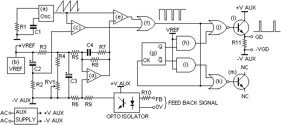
Driving the power stages and taking care of regulation is the control circuit shown above, which shows a simplified circuit to illustrate the fundamentals of operation. The control circuit itself requires power to operate, and this is provided by the block designated 'Aux. Supply'. The auxiliary supply may take several forms, and in this instance it derives its power from the 240V AC mains supply input to provide the low voltage auxiliary supply. The circuitry required to perform the control functions will normally be in the form of an integrated circuit. In figure 15b the blocks labelled with a letter ('a' to 'm') are contained in an integrated circuit, whilst the other discrete components are external to the device. Block 'a' is a highly stable oscillator which produces a sawtooth waveform, timing components R1 and C1 set the operating frequency. A stable reference voltage (VREF) is provided by block 'b', this is used by the error amplifier and other circuitry. Control of the output pulse width is under control of the Dead Time Comparator, 'c', and the Pulse Width Modulator (PWM) Comparator, 'e'. These two comparators each compare a control voltage with the sawtooth oscillator waveform. The output of the two comparators is ORed together, 'f', before being fed to the output control circuitry. The Dead Time Control Comparator is used to provide a 'soft start'; this brings the output of the power supply up to its working level over a short period of time (50ms) after switch on. This reduces stress on the components in the power stages at switch-on. The time constant for the 'soft start' is provided by R2 and C2. The Error Amplifier, 'd', is responsible for comparing the output voltage of the power supply with a reference. If the output voltage tries to deviate from its correct value, because of changes in either load and/or line voltage, the error amplifier output changes to maintain the correct output voltage. The voltage at the output of the power supply is monitored at the point marked 'FB' on Figure 15a, this voltage is coupled to the error amplifier circuitry via an Opto Isolator (Figure 15b). The Opto Isolator is required to maintain isolation between the low voltage output and the live power stages. The opto isolation circuitry has been shown as a block for clarity. The output from the Opto Isolator is fed to the non-inverting input of the Error Amplifier via a potential divider, R6 and R9, where it is compared to the reference voltage provided by another potential divider, R3, R4 and RV1. RV1 serves to adjust the output voltage of the power supply to the required level. C3 decouples the reference voltage. The gain of the error amplifier is set by the network of components, R5, R8, C4 and R7. The error amplifier is essentially a non-inverting operational amplifier circuit with the low frequency gain being set by R5 and R8.
Error Amplifier LF Gain = 1 + (R8/R5)
The combination of inductive and capacitive components in the power stages will cause phase shift, and at certain frequencies it is a possibility that the feedback loop could become unstable and break into oscillation, which is, to say the least, highly undesirable! The answer to this is to provide frequency/phase compensation; this is provided by C4 and R7. As the frequency rises, the gain of the amplifier is reduced, thus ensuring stability. The gain of the error amplifier at a given frequency is thus:
(where f is the frequency)
Impedance of frequency compensation network:
Xc = 1/(2 x pi x f x C4)
Z = (R7^2 + Xc^2)^0.5
Total Feedback Impedance:
Zf = (Z x R8) / (Z + R8)
Error Amplifier Gain at Frequency f = 1 + (Zf/R5)
The integrated circuit used in this example has two outputs, and can be 'programmed' to use these for either push-pull or single ended applications. Selection of the required mode is achieved by taking the inputs of the two AND gates (h) and (i) to either VREF for push-pull or 0V for single ended. When in push-pull mode, the frequency of the drive signal is half that of the oscillator, this is due to the action of bistable (g). The bistable ensures that the two output transistors (l) and (m) never conduct together and that the duty cycle of each drive signal never exceeds 50%. The 50% maximum is a requirement in this type of forward converter power supply. For this reason the push-pull mode is selected, even though only one output transistor (l) is used. NOR gates (j) and (k) steer the PWM drive signal to the output transistor under the control of the bistable outputs. R11 provides an emitter load for the output transistor.
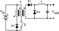
A switch mode power supply that gives a low voltage isolated output from a mains source is often referred to as an 'Off-Line SMPS'. A typical block diagram of such a supply is shown below:
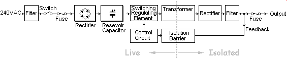
The filter shown on the left of the diagram is necessary to prevent the supply from causing interference on the mains wiring. It can also help to protect the SMPS circuitry from voltage spikes (or power surges) on the mains supply.
The filter shown on the left of the diagram is necessary to prevent the supply from causing interference on the mains wiring. It can also help to protect the SMPS circuitry from voltage spikes (or power surges) on the mains supply.
A typical power section of such a circuit is shown below:
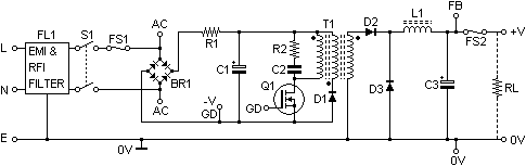
The resevoir capacitor potential would be approximately 340V for a 240V mains supply. This type of supply is sometimes designed to be powered from either 120V or 240V mains. The SMPS is set for the appropriate voltage with either a switch or a wire link. The switch activates a capacitive voltage doubling circuit when set for 120V. Resistor R1 is a low value resistor of 2 to 4 ohms which protects the circuit from the current surge that would otherwise occur at switch-on as C1 is charged. Q1 is a high voltage power MOSFET that is used as a high speed switch to supply current pulses to the ferrite cored, high frequency transformer T1. The frequency of switching is typically in the range 25 to 250kHz. R2 and C2 form a snubber network to reduce voltage spikes and switching noise. Regulation is achieved by monitoring the output voltage at the point marked 'FB' and adjusting the pulse width of the Q1 gate drive. Fuse FS2 is for short-circuit \ overload protection. FS2 is sometimes replaced by a current sensing circuit which will shut the drive circuitry down in the event of excess current.
In a mains-driven linear power supply, a mains frequency power transformer is used for isolation, and then a rectifier and linear regulator are used to provide the output voltage.
In a mains-driven SMPS, isolation, regulation and high-efficiency are combined into one. The SMPS uses a less bulky high frequency transformer typically operating at 25kHz to 250kHz (though low-power operation up to 1MHz is not unheard of).
The transformers and inductors used for SMPSs have ferrite dust cores as opposed to the laminated iron cores of their lower frequency counterparts. SMPS tranformers generally have fewer turns in the windings than the mains frequency transformers.
Switch mode power supplies are notorious for creating rfi and emi. Lowpass filters in the mains leads are vital to reduce conducted interference. Faraday screens between the transformer windings and around sensitive components, together with correct field cancelling layouts on the circuit board, are also required to reduce e.m.i. and r.f.i. The problems of smoothing of sawtooth current waveforms puts a strain on capacitor design. The series inductance and resistance of standard electrolytic capacitors has a large effect on residual ripple and noise voltages at the outputs. For low powers and very low ripple and noise levels at the outputs, linear supplies cannot be beaten. That is the main reason they hold their own there.
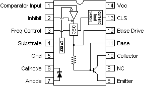
The TL497 has an osillator with a fixed on-time, but variable frequency output. This gives minimal external component count. The switch-on time is controlled by the value of a capacitor connected between pin 3 and ground.
In switch-Mode Power Supplies the 'hiccup' mode is often used for limiting output current. If an overload occurs, the circuit turns off. After an interval it comes on - has a look, as it were; if the overload is still present, it immediately goes off again. In some designs, this happens a few times, and the supply then shuts down permanently until the overload is removed and the circuit reset.
Most offline switchers are designed to maintain a steady output over a few cycles of lost mains input. This can be achieved by sizing the input capacitor such that its voltage will not fall significantly during the power interruption. The time period over which the SMPS is capable of maintaining an output when mains power is lost is frequently known as 'hold up time'.