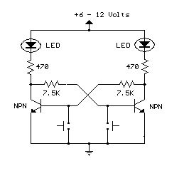
Set/Reset Flip Flop
This is an example of a set/reset flip flop using discrete components.
When power is applied, only one of the transistors will conduct causing
the other to remain off. The conducting transistor can be turned off by
grounding it's base through the push button which causes the collector
voltage to rise and turn on the opposite transistor.
Menu
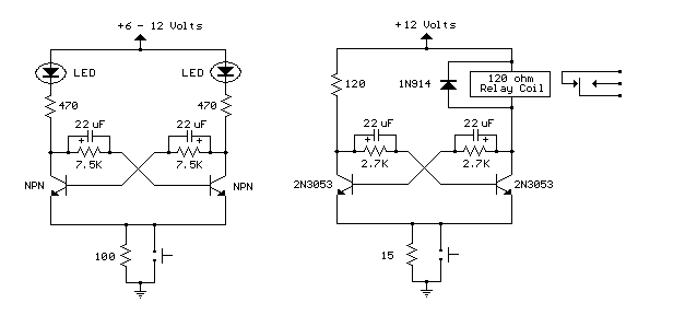
Bistable Flip Flop
Here are two examples of bistable flip flops which can be toggled
between states with a single push button. When the button is pressed,
the capacitor connected to the base of the conducting transistor will
charge to a slightly higher voltage. When the button is released, the
same capacitor will discharge back to the previous voltage causing the
transistor to turn off. The rising voltage at the collector of the
transistor that is turning off causes the opposite transistor to turn
on and the circuit remains in a stable state until the next time the
button is pressed and released. Note that in the LED circuit, the base
current from the conducting transistor flows through the LED that
should be off, causing it to illuminate dimly. The base current is
around 1 mA and adding a 1K resistor in parallel with the LED
will reduce the voltage to about 1 volt which should be low enough
to ensure the LED turns completely off.
Menu
CMOS Toggle Flip Flop With Switch Debounce
The circuit below uses a CMOS dual D flip flop (CD4013) to toggle
a relay or other load with a momentary push button. Several push buttons
can be wired in parallel to control the relay from multiple locations.
A high level from the push button is coupled to the set line through a
small (0.1uF) capacitor. The high level from the Q output is inverted by
the upper transistor and supplies a low reset level to the reset line for
about 400 mS, after which time the reset line returns to a high state and
resets the flip flop. The lower flip flop section is configured for toggle
operation and changes state on the rising edge of the clock line or at the
same time as the upper flip flop moves to the set condition. The switch is
debounced due to the short duration of the set signal relative to the
long duration before the circuit is reset. The Q or Qbar outputs
will only supply about 2 mA of current, so a buffer transistor or power
MOSFET is needed to drive a relay coil, or lamp, or other load. A 2N3904
or most any small signal NPN transistor can be used for relay coil resistances
of 250 ohms or more. A 2N3053 or medium power (500 mA) transistor should be
used for coil resistances below 250 ohms. The 47 ohm resistor and 10uF
capacitor serve to decouple the circuit from the power supply and filter out
any short duration noise signals that may be present. The RC network (.1/47K)
at the SET line (pin 8) serves as a power-on reset to ensure the relay is
denergized when circuit power is first applied. The reset idea was suggested
by Terry Pinnell who used the circuit to control a shed light from multiple
locations.

Menu
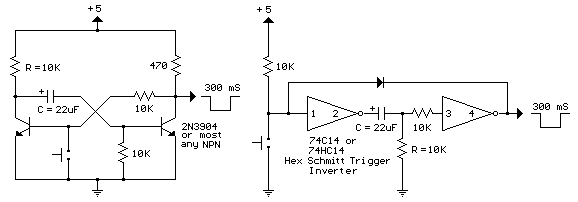
Monostable Flip Flop
The monostable flip flop, sometimes called a 'one shot' is used to
produce a single pulse each time it is triggered. It can be used
to debounce a mechanical switch so that only one rising and one
falling edge occurs for each switch closure, or to produce a delay
for timing applications. In the discrete circuit, the left
transistor normally conducts while the right side is turned off.
Pressing the switch grounds the base of the conducting transistor
causing it to turn off which causes the collector voltage to rise.
As the collector voltage rises, the capacitor begins to charge
through the base of the opposite transistor, causing it to switch
on and produce a low state at the output. The low output state holds
the left transistor off until the capacitor current falls below what
is needed to keep the output stage saturated. When the output side
begins to turn off, the rising voltage causes the left transistor
to return to it's conducting state which lowers the voltage at it's
collector and causes the capacitor to discharge through the 10K
resistor (emitter to base). The circuit then remains in a stable
state until the next input.
The one shot circuit on the right employs two logic inverters which
are connected by the timing capacitor. When the switch is closed or
the input goes negative, the capacitor will charge through the resistor
generating an initial high level at the input to the second inverter
which produces a low output state. The low output state is connected
back to the input through a diode which maintains a low input after
the switch has opened until the voltage falls below 1/2 Vcc at pin 3
at which time the output and input return to a high state. The capacitor
then discharges through the resistor (R) and the circuit remains in a stable
state until the next input arrives. The 10K resistor in series with the
inverter input (pin 3) reduces the discharge current through the input
protection diodes. This resistor may not be needed with smaller capacitor
values.
Note: These circuits are not re-triggerable and the output duration
will be shorter than normal if the circuit is triggered before the
timing capacitors have discharged which requires about the same amount
of time as the output. For re-triggerable circuits, the 555 timer,
or the 74123 (TTL), or the 74HC123 (CMOS) circuits can be used.
Menu
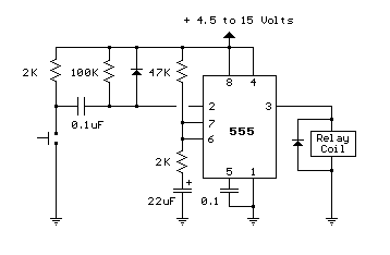
555 timer Mono stable (one shot) circuit
The circuit below illustrates using the 555 timer to close a
relay for a predetermined amount of time by pressing a momentary
N/O push button. In the idle state, the output at pin 3 will be
at ground and the relay deactivated. Pin 2, the trigger input is
held high by the 100K resistor and the both capacitors are discharged.
When the button is closed, the 0.1uF cap will charge through the
button and the 100K resistor which causes the voltage at pin 2 to move
low for a few milliseconds. The falling voltage at pin 2 triggers the
555 and starts the timing cycle. The output at pin 3 immediately moves
up to near the supply voltage (about 10.4 volts for a 12 volt supply)
and remains at that level until the 22uF timing capacitor charges
to about 2/3 of the supply voltage (about 1 second as shown).
Most 12 volt relays will work at 10.4 volts, but if not, the supply voltage
could be raised to 13.5 or so to compensate. The 555 output will supply
up to 200mA of current, so the relay could be replaced with a small lamp,
doorbell, or other load that requires less than 200mA. When the button is
released, the 0.1uF capacitor discharges through the 100K and 2K resistors.
The diode across the 100K resistor prevents the voltage at pin 2 from rising
above the supply voltage when the cap discharges. The 2K resistor in series
with the 22uF cap limits the discharge current from pin 7 of the timer.
This resistor may not be necessary, but it's a good idea to limit current
when discharging capacitors across switch contacts or transistors.
Menu
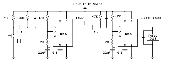
Generating a Delayed Pulse Using The 555 Timer
The circuit below illustrates generating a single positive pulse which
is delayed relative to the trigger input time. The circuit is similar to
the one above but employs two stages so that both the pulse width and
delay can be controlled. When the button is depressed, the output of
the fist stage will move up and remain near the supply voltage until
the delay time has elapsed, which in this case is about 1 second. The
second 555 stage will not respond to the rising voltage since it requires
a negative, falling voltage at pin 2, and so the second stage output
remains low and the relay remains de-energized. At the end of the delay
time, the output of the first stage returns to a low level, and the falling
voltage causes the second stage to begin it's output cycle which is also
about 1 second as shown. This same circuit can be built using the dual
555 timer which is a 556, however the pin numbers will be different.
Menu
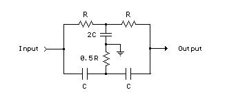
RC Notch Filter (Twin T)
The twin T notch filter can be used block an unwanted frequency or
if placed around an op-amp as a bandpass filter. The notch frequency
occurs where the capacitive reactance equals the resistance (Xc=R)
and if the values are close, the attenuation can be very high and the
notch frequency virtually eliminated. The insertion loss of the filter
will depend on the load that is connected to the output, so the resistors
should be of much lower value than the load for minimal loss. At audio
frequencies, the filter could function as a bass and treble boost circuit
by attenuating the mid range frequencies. Using 1.5K resistors and 0.1uF
capacitors, the band stop at -10dB is about 500 Hz to 2Khz. The depth and
width of the response can be adjusted somewhat with the 0.5R value and
by adding some resistance across the C values. If the circuit is used
around an op-amp as a bandpass filter, the response may need to be
dampened to avoid oscillation.
Menu
�