| This version reflects the comments of the core participants as reviewed and incorporated in accordance with CORD's FIPSE-supported Curriculum Morphing Project. | |||||
MODULE 4-8 (1) The detection of optical radiation is usually accomplished by converting the optical energy into an electrical signal. Optical detectors include photon detectors, in which one photon of light energy releases one electron that is detected in the electronic circuitry, and thermal detectors, in which the optical energy is converted into heat, which then generates an electrical signal. Often the detection of optical energy must be performed in the presence of noise sources, which interfere with the detection process. The detector circuitry usually employs a bias voltage and a load resistor in series with the detector. The incident light changes the characteristics of the detector and causes the current flowing in the circuit to change. The output signal is the change in voltage drop across the load resistor. Many detector circuits are designed for specific applications.
When you complete this unit, you will be able to: 1. Define detector responsivity, noise equivalent power, quantum efficiency, detectivity, and rise time. 2. Define sources of detector noise, including shot noise, Johnson noise, 1/f noise, and photon noise. Explain methods employed to reduce these noise sources in the detection of optical radiation. 3. Describe and explain important types of photodetectors, including photon detectors, thermal detectors, photoemissive detectors, photoconductive detectors, photovoltaic detectors, and photomultiplier detectors. Describe the spectral response of each type. 4. Draw and explain circuitry used with photomultiplier detectors. 5. Draw and explain photodiode circuits for use in the photoconductive and photovoltaic modes of operation. 6. Fabricate a circuit for operation of a photodiode and use it for detection of light in both photoconductive and photovoltaic modes of operation.  Light Detection
(2) When light strikes special types of materials, a voltage may be generated, a change in electrical resistance may occur, or electrons may be ejected from the material surface. As long as the light is present, the condition continues. It ceases when the light is turned off. Any of the above conditions may be used to change the flow of current or the voltage in an external circuit, and hence may be used to monitor the presence of the light and to measure its intensity. (3) Detectors suitable for monitoring optical power or energy are commonly employed along with lasers and other light sources. For an application such as laser communication, a detector is necessary as the receiver. For applications involving interferometry, detectors are used to measure the position and motion of the fringes in the interference pattern. In applications involving laser material processing, a detector monitors the laser output to ensure reproducible conditions. In very many applications of light, one desires a detector to determine the output of the laser or other light source. Thus, good optical detectors for measuring optical power and energy are essential. (4) All optical detectors respond to the power in the optical beam, which is proportional to the square of the electric field. They are thus called "square-law detectors." Microwave detectors, in contrast, can measure the electric field intensity directly. But all the detectors that we consider here exhibit square-law response. This is also true of other common optical detectors such as the human eye and photographic film. (5) The detection and measurement of optical and infrared radiation is a well-established area of technology. In recent years, this technology has been applied specifically to laser applications, and detectors particularly suitable for use with lasers have been developed. Commercial developments have also kept pace. Detectors specially designed and packaged for use with lasers are marketed by numerous manufacturers. Some detectors are packaged in the format of a power or energy meter. These devices include a complete system for measuring the output of a specific class of lasers, and include a detector, housing, amplification if necessary, and a readout device. (6) In this module, we will describe some of the detectors that are available. We shall not attempt to cover the entire field of light detection, which is very broad. Instead, we shall emphasize those detectors that are most commonly encountered. We shall also define some of the common terminology. (7) There are two broad classes of optical detectors: photon detectors and thermal detectors. Photon detectors rely on the action of quanta of light energy to interact with electrons in the detector material and to generate free electrons. To produce such effects, the quantum of light must have sufficient energy to free an electron. The wavelength response of photon detectors shows a long-wavelength cutoff. When the wavelength is longer than the cutoff wavelength, the photon energy is too small to liberate an electron and the response of the detector drops to zero. (8) Thermal detectors respond to the heat energy delivered by the light. The response of these detectors involves some temperature-dependent effect, like a change of electrical resistance. Because thermal detectors rely on only the amount of heat energy delivered, their response is independent of wavelength. (9) The output of photon detectors and thermal detectors as a function of wavelength is shown schematically in Figure 1. This shows how the output of thermal detectors is independent of wavelength. It also shows the typical spectral dependence of the response of photon detectors, which increases with increasing wavelength until the cutoff wavelength is reached. At that point it drops rapidly to zero.
Fig. 1 (10) Photon detectors may be further subdivided into the following groups: • Photoconductive. The electrical conductivity of the material changes as a function of the intensity of the incident light. Photoconductive detectors are semiconductor materials. They have an external electrical bias voltage. • Photovoltaic. These detectors contain a p-n semiconductor junction and are often called photodiodes. A voltage is self generated as radiant energy strikes the device. The photovoltaic detector may operate without external bias voltage. A good example is the solar cell used on spacecraft and satellites to convert the sun’s light into useful electrical power. • Photoemissive. These detectors use the photoelectric effect, in which incident photons free electrons from the surface of the detector material. These devices include vacuum photodiodes, bipolar phototubes, and photomultiplier tubes. Photoconductive and photovoltaic detectors are commonly used in circuits in which there is a load resistance in series with the detector. The output is read as a change in the voltage drop across the resistor. (11) We shall describe these effects in more detail later in the discussion of the types of detectors.
Detector Characteristics (12) The performance of optical detectors is commonly described by a number of different figures of merit, which are widely used throughout the field of optical detection. They were developed originally to describe the capabilities of a detector in responding to a small signal in the presence of noise. As such, they are not always pertinent to the detection of laser light. Often in laser applications—for example, in laser metalworking—there is no question of detection of a small signal in a background of noise. The laser signal is far larger than any other source that may be present. But in other applications, like laser communications, infrared thermal imaging systems, and detection of backscattered light in laser Doppler anemometry, the signals are small, and noise considerations are important. It is also worthwhile to define these figures of merit because the manufacturers of detectors usually describe the performance of their detectors in these terms. (13) The first term that is commonly used is responsivity. This is defined as the detector output per unit of input power. The units of responsivity are either amperes/watt (alternatively milliamperes/milliwatt or microamperes/microwatt, which are numerically the same) or volts/watt, depending on whether the output is an electric current or a voltage. This depends on the particular type of detector and how it is used. Figure 1 can be considered to be a representation of how the responsivity varies with wavelength for photon detectors and thermal detectors. We note that the responsivity gives no information about noise characteristics. (14) The responsivity is an important characteristic that is usually specified by the manufacturer, at least as a nominal value. Knowledge of the responsivity allows the user to determine how much detector signal will be available in a specific application. One may also characterize the spectral responsivity, which is the responsivity as a function of wavelength. (15) A second figure of merit, one that depends on noise characteristics, is the noise equivalent power (NEP). This is defined as the radiant power that produces a signal voltage (current) equal to the noise voltage (current) of the detector. Since the noise is dependent on the bandwidth of the measurement, that bandwidth must be specified. The equation defining NEP is NEP = IAVN/VS(D f)1/2 Equation 1 where I is the irradiance incident on the detector of area A, VN is the root mean square noise voltage within the measurement bandwidth D f, and VS is the root mean square signal voltage. The NEP has units of watts per (hertz to the one-half power), commonly called watts per root hertz. From the definition, it is apparent that the lower the value of the NEP, the better are the characteristics of the detector for detecting a small signal in the presence of noise. (16) The NEP of a detector is dependent on the area of the detector. To provide a figure of merit under standard conditions, a term called detectivity is defined. Detectivity is represented by the symbol D*, which is pronounced as D-star. It is defined by D* = A1/2/NEP Equation 2 (17) Since many detectors have NEP proportional to the square root of their area, D* is independent of the area of the detector and provides a measure of the intrinsic quality of the detector material itself, independent of the area with which the detector happens to be made. When a value of D* for a photodetector is measured, it is usually measured in a system in which the incident light is modulated or chopped at a frequency f so as to produce an AC signal, which is then amplified with an amplification bandwidth D f. The dependence of D* on the wavelength l , the frequency f at which the measurement is made, and the bandwidth D f are specified in the notation D*(l ,f,D f). The reference bandwidth is frequently taken as 1 hertz. The units of D*(l ,f,D f) are centimeters (square root hertz) per watt. A high value of D*(l ,f,D f) means that the detector is suitable for detecting weak signals in the presence of noise. Later, in the discussion of noise, we will describe the effect of the modulation frequency and the bandwidth on the noise characteristics. (18) Another commonly encountered figure of merit for photodetectors is the quantum efficiency. Quantum efficiency is defined as the ratio of countable events produced by photons incident on the detector to the number of photons. If the detector is a photoemissive detector that emits free electrons from its surface when light strikes it, the quantum efficiency is the number of free electrons divided by the number of incident photons. If the detector is a semiconductor p-n junction device in which hole-electron pairs are produced, the quantum efficiency is the number of hole-electron pairs divided by the number of incident photons. Thus if, over a period of time, 100,000 photons are incident on the detector and 10,000 hole-electron pairs are produced, the quantum efficiency is 10%. (19) The quantum efficiency is basically another way of expressing the effectiveness of the incident radiant energy for producing electrical current in a circuit. It may be related to the responsivity by the equation: Q = 100 ´ Rd ´ hv = 100 ´ Rd ´ (1.2395/l ) Equation 3 where Q is the quantum efficiency (in %) and Rd is the responsivity (in amperes per watt) of the detector at wavelength l (in micrometers), and hv is the photon energy. The right portion of the equation makes calculation easy for a specific responsivity at a given wavelength. (20) Another important detector characteristic is the speed of the detector response to changes in light intensity. If a constant source of light energy is instantaneously turned on and irradiates a photodetector, it will take a finite time for current to appear at the output of the device and for the current to reach a steady value. If the same source is turned off instantaneously, it will take a finite time for the current to decay back to its initial zero value. The term response time generally refers to the time it takes the detector current to rise to a value equal to 63.2% of the steady-state value reached after a relatively long period of time. (This value is numerically equal to 1- 1/e, where e is the base of the natural logarithms.) The recovery time is the time photocurrent takes to fall to 36.8% of the steady-state value when the light is turned off instantaneously. (21) Because photodetectors often are used for detection of fast pulses, a more important term, called rise time, is often used to describe the speed of the detector response. Rise time is defined as the time difference between the points at which the detector has reached 10% of its peak output and the point at which it has reached 90% of its peak response, when it is irradiated by a very short pulse of light. The fall time is defined as the time between the 90% point and the 10% point on the trailing edge of the pulse waveform. This is also called the decay time. We note that the fall time may be different numerically from the rise time. (22) Of course light sources are not turned on or off instantaneously. For accurate measurements of rise time and fall time, the source used for the measurement should have a rise time much less that the rise time of the detector that is being tested. Generally one will accept a source whose rise time is less than 10% of the rise time of the detector being tested. (23) Other factors that affect measured rise times are the limitations introduced by the electrical cables and by the display device, for example, the oscilloscope or recorder. These devices can make the measured rise time appear longer than the value that arises from the detector alone. (24) The response time of a photodetector arises from the transit time of photogenerated charge carriers within the detector material and from the inherent capacitance and resistance associated with the device. It is also affected by the value of the load resistance that is used with the detector. There is a tradeoff in the selection of a load resistance between speed of response and high sensitivity. It is not possible to achieve both simultaneously. Fast response requires a low load resistance (generally 50 ohms or less), whereas high sensitivity requires a high value of load resistance. It is also important to keep any capacitance associated with the circuitry or display device as low as possible. This will help to keep the RC time constant low. (25) Manufacturers often quote nominal values for the rise times of their detectors. These should be interpreted as minimum values, which may be achieved only with careful circuit design and avoidance of excess capacitance and resistance. (26) Another important characteristic of detectors is their linearity. Photodetectors are characterized by a response that is linear with incident intensity over a broad range, perhaps many orders of magnitude. If the output of the detector is plotted versus the input power, there should be no change in the slope of the curve. Noise will determine the lowest level of incident light that is detectable. The upper limit of the input/output linearity is determined by the maximum current that the detector can handle without becoming saturated. Saturation is a condition in which there is no further increase in detector response as the input light is increased. Linearity may be quantified in terms of the maximum percentage deviation from a straight line over a range of input light levels. For example, the maximum deviation from a straight line could be 5% over the range of input light from 10- 12 W/cm2 to 10- 4 W cm2. One would state that the linearity is 5% over eight orders of magnitude in the input. (27) The manufacturer often specifies a maximum allowable continuous light level. Light levels in excess of this maximum may cause saturation, hysteresis effects, and irreversible damage to the detector. If the light occurs in the form of a very short pulse, it may be possible to exceed the continuous rating by some factor (perhaps as much as 10 times) without damage or noticeable changes in linearity.
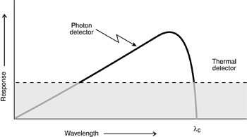
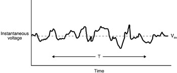
Noise Considerations (28) The topic of noise in optical detectors is a complex subject. In this module we will do no more than present some of the most basic ideas. Noise is defined as any undesired signal. It masks the signal that is to be detected. Noise can be distinguished as external and internal. External noise involves those disturbances that appear in the detection system because of actions outside the system. Examples of external noise could be pickup of hum induced by 60-Hz electrical power lines and static caused by electrical storms. Internal noise includes all noise generated within the detection system itself. Every electronic device has internal sources of noise, which may be considered as an ever-present limit to the smallest signal that may be handled by the system. (29) Noise cannot be described in the same manner as usual electric currents or voltages. We think of currents or voltages as functions of time, such as constant direct currents or sine-wave alternating voltages. The noise output of an electrical circuit as a function of time is completely erratic. We cannot predict what the output will be at any instant. There will be no indication of regularity in the waveform. The output is said to be random. (30) The output from a random noise generator might look like what is shown in Figure 2, which is a plot of instantaneous voltage as a function of time. Because of the random nature of the noise, the voltage fluctuates about an average value Vav. How does one describe these variations? A simple average is meaningless because the average is zero. Rather, one uses an average of the squares of the deviations around Vav, with the average taken over a period of time T much longer than the period of the fluctuations.
Fig. 2
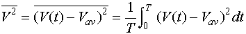
Mathematically this is expressed as:
where v(t) is the value of the voltage at time t and (31) The right side of the equation contains an integral sign with limits 0 and T. This means that one adds all values (v(t) – Vav)2 for each small increment of time Dt in the interval from time 0 to time T. It is unlikely that one would calculate the noise voltage directly from this equation, because the process would be laborious. The equation does define the basic concept. (32) If two or more noise sources are present, their total effect is found by adding their mean square voltages. Since mean square voltages are proportional to power, this is equivalent to saying that noise powers are additive, but noise voltages or currents are not. As an example, if two independent noise sources are present in a circuit, with root-mean-square (rms) noise voltages of 30 and 40 microvolts, the total rms noise voltage is (302 + 402)1/2 or 50 microvolts. (33) Now we will consider some of the sources of noise encountered in optical detector applications. A complete description of all types of noise would be very long. We will describe the four types most often encountered in a system for visible and infrared detection: • Johnson noise • Shot noise • 1/f noise • Photon noise (34) Johnson noise is a type of noise generated by thermal fluctuations in conducting materials. It is sometimes called thermal noise. It results from the random motion of electrons in a conductor. The electrons are in constant motion, colliding with each other and with the atoms of the material. Each motion of an electron between collisions represents a tiny current. The sum of all these currents taken over a long period of time is zero, but their random fluctuations over short intervals constitute Johnson noise. (35) The mean square value of the voltage associated with Johnson noise is:
where K is Boltzmann’s constant (1.38 ´ 10- 23 joule/degree Kelvin), T is the absolute temperature, R is the circuit resistance (ohms), and D f is the bandwidth of the amplification (Hz). Since the load resistance is usually greater than the internal resistance of the photodetector, the Johnson noise may be dominated by the load resistor. This equation is also frequently written as V2 = 4KTRB, with B denoting the bandwidth. (36) The equation indicates methods to reduce the magnitude of the Johnson noise. One may cool the system, especially the load resistor. One should reduce the value of the load resistance, although this is done at the price of reducing the available signal. One should keep the bandwidth of the amplification small; one Hz is a commonly employed value. (37) The term shot noise is derived from fluctuations in the stream of electrons in a vacuum tube. These variations create noise because of the random fluctuations in the arrival of electrons at the anode. It originally was likened to the the noise of a hail of shot striking a target; hence the name shot noise was applied. In semiconductors, the major source of noise is due to random variations in the rate at which charge carriers are generated and recombine. This noise, called generation-recombination or gr noise, is the semiconductor counterpart of shot noise. The mean-square current fluctuation for shot noise in a semiconductor photodetector is:
where e is the electronic charge (1.6 ´ 10- 19 coulomb), IDC is the DC component of dark leakage current (or any current) in amperes, and D f is the bandwidth of the amplification (Hz). Note that here we have specified a mean square noise current, instead of a voltage. (38) The shot noise may be minimized by keeping any DC component to the current small, especially the dark current, and by keeping the bandwidth of the amplification system small. (39) The term 1/f noise (pronounced one over f) is used to describe a number of types of noise that are present when the modulation frequency f is low. This type of noise is also called excess noise because it exceeds shot noise at frequencies below a few hundred Hertz. With respect to photodiodes, it is sometimes called boxcar noise, because it can suddenly appear and then disappear in small boxes of noise observed over a period of time. (40) The mechanisms that produce 1/f noise are poorly understood and there is no simple mathematical expression to define 1/f noise. The noise power is inversely proportional to f, the modulation frequency. This dependence of the noise power leads to the name for this type of noise. (41) To reduce 1/f noise, a photodetector should be operated at a reasonably high frequency, often taken as 1000 Hz. This is a high enough value to reduce the contribution of 1/f noise to a small amount. Since to reduce Johnson noise and shot noise, the amplification bandwidth should be small (perhaps 1 Hz), measurements of the spectral detectivity are often expressed as D*(l ,1000,1). (42) Even if all the previously discussed sources of noise could be eliminated, there would still be some noise present in the output of a photodetector because of the random arrival rate of photons from the source of radiant energy that is being measured and from the background. This contribution to the noise is called photon noise, and is a noise source external to the detector. It imposes the ultimate fundamental limit to the detectivity of a photodetector. (43) The photon noise associated with the fluctuations in the arrival rate of photons in the desired signal is not something that can be reduced. The contribution of fluctuations in the arrival of photons from the background, a contribution that is called background noise, can be reduced. The background noise increases with the field of view of the detector and with the temperature of the background. In some cases it may be possible to reduce the field of view of the detector so as to view only the source of interest. In other cases it may be possible to cool the background. Both these measures may be used to reduce the background noise contribution to photon noise. (44) Any of the types of noise described here, or a combination of the noise powers from a combination of the sources, will set an upper limit to the detectivity of a photodetector system.
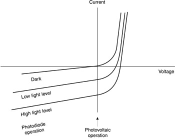
Types of Detectors Photon Detectors (45) We have previously distinguished photon detectors and thermal detectors. We begin the detailed discussion of detector types with photon detectors. As mentioned before, photon detectors rely on liberating free electrons and require the photon to have sufficient energy to exceed some threshold, i.e., the wavelength must be shorter than the cutoff wavelength. We will consider three types of photoeffect that are often used for detectors. These are the photovoltaic effect, the photoemissive effect, and the photoconductive effect. (46) The photovoltaic effect and the operation of photodiodes both rely on the presence of a p-n junction in a semiconductor. When such a junction is in the dark, an electric field is present internally in the junction region because there is a change in the level of the conduction and valence bands. This change leads to the familiar electrical rectification effect produced by such junctions. (47) When light falls on the junction, it is absorbed and, if the photon energy is large enough, it produces free hole-electron pairs. The electric field at the junction separates the pair and moves the electron into the n-type region and the hole into the p-type region. This leads to a change in voltage that may be measured externally. This process is the origin of the so-called photovoltaic effect. The photovoltaic effect is the generation of a voltage when light strikes a semiconductor p-n junction. We note that the open-circuit voltage generated in the photovoltaic effect may be detected directly and that no bias voltage or ballast resistor is required. (48) It is also possible to use a p-n junction to detect light if one does apply a bias voltage in the reverse direction. By reverse direction, we mean the direction of low current flow, that is, with the positive voltage applied to the n-type material. A p-n junction detector with bias voltage is termed a photodiode. The current-voltage characteristics of a photodiode are shown in Figure 3. The curve labeled "dark" represents conditions in the absence of light; it displays the familiar rectification characteristics of a p-n semiconductor diode. The other curves show the current-voltage characteristics when the device is illuminated at different light levels. The characteristics of a photovoltaic detector, with zero applied voltage, are represented by the intersections of the different curves with the vertical axis. The photodiode detector is operated in the lower left quadrant of this figure. The current that may be drawn through an external load resistor increases with increasing light level. In practice, one measures the voltage drop appearing across the resistor.
Fig. 3 (49) To increase the frequency response of photodiodes, a type called the PIN photodiode has been developed. This device has a layer of nearly intrinsic material bounded on one side by a relatively thin layer of highly doped p-type semiconductor, and on the other side by a relatively thick layer of n-type semiconductor. A sufficiently large reverse bias voltage is applied so that the depletion layer, from which free carriers are swept out, spreads to occupy the entire volume of intrinsic material. This volume then has a high and nearly constant electric field. It is called the depletion region because all mobile charges have been removed. Light that is absorbed in the intrinsic region produces free electron-hole pairs, provided that the photon energy is high enough. These carriers are swept across the region with high velocity and are collected in the heavily doped regions. The frequency response of such PIN photodiodes can be very high, of the order of 1010 Hz. This is higher than the frequency response of p-n junctions without the intrinsic region. (50) A variety of photodiode structures is available. No single photodiode structure can best meet all system requirements. Therefore, a number of different types has been developed. These include the planar diffused photodiode, shown if Figure 4a, and the Schottky photodiode, shown in Figure 4b. The planar diffused photodiode is formed by growing a layer of oxide over a slice of high-resistivity silicon, etching a hole in the oxide, and diffusing boron into the silicon through the hole. This structure leads to devices with high breakdown voltage and low leakage current. The circuitry for operation of the photodiode is also indicated, including the load resistor RL.
Fig. 4 (51) The Schottky barrier photodiode uses a junction between a metallic layer and a semiconductor. If the metal and the semiconductor have work functions related in the proper way, this can be a rectifying barrier. The junction is formed by oxidation of the silicon surface, etching of a hole in the oxide, and then evaporation of a thin transparent and conducting gold layer. The insulation guard rings serve to reduce the leakage current through the devices. (52) A number of different semiconductor materials is in common use as optical detectors. They include silicon in the visible and near ultraviolet and near infrared, germanium and indium gallium arsenide in the near infrared, and indium antimonide, indium arsenide, mercury cadmium telluride, and germanium doped with elements like copper and gold in the longer-wavelength infrared. (53) The most frequently encountered type of photodiode is silicon. Silicon photodiodes are widely used as the detector elements in optical disks and as the receiver elements in optical-fiber telecommunication systems operating at wavelengths around 800 nm. Silicon photodiodes respond over the approximate spectral range of 400-1100 nm, covering the visible and part of the near-infrared regions. The spectral responsivity of typical commercial silicon photodiodes is shown in Figure 5. The responsivity reaches a peak value around 0.7 amp/watt near 900 nm, decreasing at longer and shorter wavelengths. Optional models provide somewhat extended coverage in the infrared or ultraviolet regions. Silicon photodiodes are useful for detection of many of the most common laser wavelengths, including argon, He-Ne, AlGaAs, and Nd:YAG. As a practical matter, silicon photodiodes have become the detector of choice for many laser applications. They represent well-developed technology and are widely available. They represent the most widely used type of laser detectors for lasers operating in the visible and near-infrared portions of the spectrum.
Fig. 5 (54) Other types of photodetectors are available for detection of light in other wavelength regions. Photodetectors have been fabricated from many other materials. Different detector materials are useful in different spectral regions. Figure 6 shows the spectral D* (or detectivity) for a number of commercially available detectors operating in the infrared spectrum. The figure includes both photovoltaic detectors and photoconductive detectors, which will be described in more detail later. The choice of detector will depend on the wavelength region that is desired. For example, for a laser operating at 5 mm, an indium antimonide photovoltaic detector would be suitable.
Fig. 6
(55) The shape of the curves in Figure 6 is characteristic of photon detectors. One photon produces one electron-hole pair in the material, so long as the photon energy is high enough. Absorption of one photon then gives a constant response, independent of wavelength (provided that the wavelength lies within the range of spectral sensitivity of the detector). One photon of ultraviolet light and one photon of infrared light each produces the same result, even though they have much different energy. For constant photon arrival rate, as wavelength increases, the incident power decreases, but the response remains the same. Therefore, the value of D* increases, reaching a maximum at the cutoff wavelength, which is equal to the Planck’s constant times the velocity of light divided by the band gap of the material. At longer wavelengths, the detectivity decreases rapidly because the photons do not have enough energy to excite an electron into the conduction band. (56) Figure 6 also indicates the detectivity for "ideal" detectors, that is, detectors whose performance is limited only by fluctuations in the background of incident radiation, and that do not contribute noise themselves. Available detectors approach the ideal performance limits fairly closely. (57) Another variation of the photodiode is the avalanche photodiode. The avalanche photodiode offers the possibility of internal gain; it is sometimes referred to as a "solid-state photomultiplier." The most widely used material for avalanche photodiodes is silicon, but they have been fabricated from other materials, such as germanium. An avalanche photodiode has a diffused p-n junction, with surface contouring to permit high reverse-bias voltage without surface breakdown. A large internal electric field leads to multiplication of the number of charge carriers through ionizing collisions. The signal is thus increased, to a value perhaps 100-200 times greater than that of a nonavalanche device. The detectivity is also increased, provided that the limiting noise is not from background radiation. Avalanche photodiodes cost more than conventional photodiodes, and they require temperature-compensation circuits to maintain the optimum bias, but they represent an attractive choice when high performance is required. (58) Silicon and other photodiodes have been configured as power meters, whicH are calibrated so that the detector output may be presented on a display as the laser power. These devices may be used directly to measure the power of a continuous laser or of a repetitively pulsed laser operating at a reasonably high pulse-repetition rate. Some commercial units can measure powers down to the nanowatt regime. Because the photodiode response varies with wavelength, the manufacturer usually supplies a calibration graph to allow conversion to wavelengths other than that for which the photodiode was calibrated. Alternatively, some units are supplied with filters to compensate for the wavelength variation of the detector response, so that the response of the entire unit will be wavelength-independent, at least over some interval. Such packaged power meters provide a convenient and useful monitor of laser output power. (59) A photoemissive detector employs a cathode coated with a material that emits electrons when light of wavelength shorter than a certain value falls on the surface. The electrons emitted from the surface may be accelerated by a voltage to an anode where they give rise to a current in an external circuit. These detectors are available commercially from a number of manufacturers. They represent an important class of detectors for many applications. (60) Some standardized spectral response curves for photoemissive cathodes are shown in Figure 7. The materials have low work functions, that is, incident light may easily cause the surfaces to emit an electron. The cathodes are often mixtures containing alkali metals, such as sodium and potassium. The usefulness of these devices ranges from the ultraviolet to the near infrared. At wavelengths longer than 1.2 m m, no photoemissive response is available. The short-wavelength end of the response curve is set by the nature of the window material used in the tube that contains the detector. The user can select a device with a cathode with maximum response in a selected wavelength region.
Fig. 7
(61) An important variation of the photoemissive detector is the photomultiplier. This is a device with a photoemissive cathode and a number of secondary emitting stages called dynodes. The dynodes are arranged so that electrons from each dynode are delivered to the next dynode in the series. Electrons emitted from the cathode are accelerated by an applied voltage to the first dynode, where their impact causes emission of numerous secondary electrons. These electrons are accelerated to the next dynode and generate even more electrons. Finally, electrons from the last dynode are accelerated to the anode and produce a large current pulse in the external circuit. The photomultiplier is packaged as a vacuum tube. (62) Figure 8 shows a cross-sectional diagram of a typical photomultiplier tube structure. This tube has a transparent end window with the underside coated with the photocathode material. Figure 9 shows the principles of operation of the tube. With careful design, photoelectrons emitted from the cathode will strike the first dynode, where they produce 1 to 8 secondary electrons per incident electron. These are accelerated to the second dynode, where the process is repeated. After several such steps the electrons are collected at the anode and flow through the load resistor. Voltages of 100 to 300 volts are required to accelerate electrons between dynodes, so that the total tube voltage may be from 500 to 3000 volts from anode to cathode, depending on the number of dynodes.
Fig. 8
Fig. 9
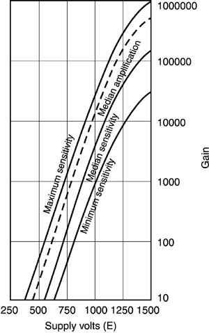
(63) The current gain of a photomultiplier is defined as the ratio of anode current to cathode current. Typical values of gain may be in the range 100,000 to 1,000,000. Thus 100,000 or more electrons reach the anode for each photon striking the cathode. Figure 10 shows a plot of gain as a function of the voltage from the anode to the cathode, for a typical photomultiplier tube. This high gain process means that photomultiplier tubes offer the highest available responsivity in the ultraviolet, visible, and near-infrared portions of the spectrum. Photomultiplier tubes can in fact detect the arrival of a single photon at the cathode. Applications of photomultiplier tubes include scintillation counting, air-pollution monitoring, photon counting, star tracking, photometry, and radiometry.
Fig. 10. (64) A third class of photodetector uses the phenomenon of photoconductivity. A semiconductor in thermal equilibrium contains free electrons and holes. The concentration of electrons and holes is changed if light is absorbed by the semiconductor. The light must have photon energy large enough to cause excitation, either by raising electrons across the forbidden band gap or by activating impurities present within the band gap. The increased number of charge carriers leads to an increase in the electrical conductivity of the semiconductor. The device is used in a circuit with a bias voltage and a load resistor in series with it. The change in electrical conductivity leads to an increase in the current flowing in the circuit, and hence to a measurable change in the voltage drop across the load resistor. (65) Photoconductive detectors are most widely used in the infrared spectrum, at
wavelengths where photoemissive detectors are not available and the wavelengths are beyond
the cutoffs of the best photodiodes (silicon and germanium). Many different materials are
used as infrared photoconductive detectors. Typical values of spectral detectivity for
some common devices operating in the infrared have already been shown in (66) In its most simple form, a photoconductive detector is a crystal of semiconductor material that has low conductance in the dark and an increased value of conductance when it is illuminated. In a series circuit with a battery and a load resistor, the detector element has its conductance increased by light. The sensing of the presence of the light is accomplished via the increased voltage drop across the load resistor. But it is possible to use photodiodes in a photoconductive mode as well as in the photovoltaic mode that we have already described. (67) In Figure 3 we presented the voltage-current characteristics of p-n junction photodetectors. In the first quadrant, the device acts as a photovoltaic detector. It produces a voltage proportional to the incident light intensity. In the third quadrant, when a reverse voltage is applied, it acts as a photoconductive detector. In the dark, the reverse current is very small. When light strikes the diode, there is little increase in the forward current, but the reverse current can increase significantly. The current is proportional to the intensity of the incident light, and the increase can be linear over many orders of magnitude. (68) Figure 11 shows the voltage-current characteristics in a different way. Note that the curve has been rotated 180° from Figure 3. The photoconductive mode of operation appears on the right side of the figure. Negative values of reverse voltage increase from left to right, starting at the origin. The forward-biased (photovoltaic) device is a voltage generator. If it operates with a low-resistance load, the operation is along the near-vertical line and the current output is fairly linear with input radiation. As the load resistance increases, the output becomes nonlinear. If one observes the open-circuit voltage (load line horizontal), the open-circuit voltage is found to be proportional to the logarithm of the input light intensity.
Fig. 11 (69) In the reverse-biased or photoconductive mode, linear operation is maintained so long as the photodiode is not saturated and the bias voltage is higher than the product of the load resistance and the current. (70) For a reverse-biased device, the photodiode exhibits higher responsivity, faster response time, and greater linearity than when operated in the forward-biased mode. One drawback is the presence of a small dark current. In the forward-biased mode, the dark current may be eliminated. This makes photovoltaic devices desirable for low-level measurements in which the dark current would interfere. But the responsivity and speed decrease and the response becomes nonlinear for large values of load resistance.
Thermal detectors (71) Now we turn to the second broad class of photodetectors, thermal detectors. Thermal detectors respond to the total energy absorbed, regardless of wavelength. They have no long-wavelength cutoff in their response, as photon detectors do. The value for D* for a thermal detector is independent of wavelength. Thermal detectors generally do not offer as rapid response as photon detectors, and for laser work are not often used in the wavelength region in which photon detectors are most effective (£ 1.55 m m). They are often used at longer wavelengths. (72) Pyroelectric detectors represent one popular form of thermal detector. These detectors respond to the change in electric polarization that occurs in certain classes of crystalline materials as their temperature changes. The change in polarization, called the pyroelectric effect, may be measured as an open-circuit voltage or as a short-circuit current. The temporal response is fast enough to respond to very short laser pulses. This behavior is in contrast to that of many other thermal detectors, which tend to be slower than photon detectors. Pyroelectric detectors are often used in conjunction with CO2 lasers. (73) The calorimeter represents another type of thermal detector. Calorimetric measurements yield a simple determination of the total energy in a laser pulse, but usually do not respond rapidly enough to follow the pulse shape. Calorimeters designed for laser measurements usually use a blackbody absorber with low thermal mass with temperature-measuring devices in contact with the absorber to measure the temperature rise. Knowledge of the thermal mass coupled with measurement of the temperature rise yields the energy in the laser pulse. The temperature-measuring devices include thermocouples, bolometers, and thermistors. Bolometers and thermistors respond to the change in electrical resistivity that occurs as temperature rises. Bolometers use metallic elements; thermistors use semiconductor elements. (74) Many different types of calorimeters have been developed for measuring the total energy in a laser pulse or for integrating the output from a continuous laser. Since the total energy in a laser pulse is usually not large, the calorimetric techniques are rather delicate. The absorbing medium must be small enough that the absorbed energy may be rapidly distributed throughout the body. It must be thermally isolated from its surroundings so that the energy is not lost. (75) One form of calorimeter uses a small, hollow carbon cone, shaped so that radiation entering the base of the cone will not be reflected back out of the cone. Such a design acts as a very efficient absorber. Thermistor beads or thermocouples are placed intimately in contact with the cone. The thermistors form one element of a balanced bridge circuit, the output of which is connected to a display or meter. As the cone is heated by a pulse of energy, the resistance of the bridge changes, leading to an unbalance of the bridge and a voltage pulse that activates the display. The pulse decays as the cone cools to ambient temperature. The magnitude of the voltage pulse gives a measure of the energy in the pulse. In some designs, two identical cones are used to form a conjugate pair in the bridge circuit. This approach allows cancellation of drifts in the ambient temperature. (76) A calorimeter using a carbon cone or similar design is a simple and useful device for measurement of laser pulse energy. In the range of energy below 1 J or so, an accuracy of a few percent or better should be attainable. The main sources of error in conical calorimeters for pulsed energy measurements are loss of some of the energy by reflection, loss of heat by cooling of the entire system before the heat is distributed uniformly, and imperfect calibration. Calibration using an electrical-current pulse applied to the calorimeter element can make the last source of error small. With careful technique, the other sources of error can be held to a few percent. (77) Calorimeters using absorbing cones or disks with thermocouples to sense the temperature rise have been developed for laser pulses with energy up to hundreds of joules. When the laser energy becomes high, destructive effects, such as vaporization of the absorbing surface, may limit the usefulness of calorimeters. Since calorimeters require surface absorption of the laser energy, there are limits to the energy that a calorimeter can withstand without damage. (78) If the response of the calorimeter is fast, it can be used for measurement of power in a continuous laser beam. The temperature of the absorber will reach an equilibrium value dependent on the input power. Such units are available commercially as laser power meters, with different models capable of covering the range from fractions of a milliwatt to ten kilowatts. (79) Compared to the power meters based on silicon or other photodiodes, the power meters based on absorbing cones or disks are useful over a wider range of wavelength, and do not require use of a compensating factor to adjust for the change in response as the laser wavelength changes. Also, power meters based on these thermal detectors tend to cover a higher range of laser power than do the models based on photodiodes. (80) Some values of D* for thermal detectors are shown in Figure 12. The values are independent of wavelength. In the visible and near infrared, the values of D* for thermal detectors tend to be lower than for good photon detectors, but the response does not decrease at long wavelength.
Fig. 12 Calibration (81) The response of any photodetector in current (or voltage) per unit input of power is often taken as the nominal value specified by the manufacturer. For precise work, the detector may have to be calibrated by the user. But accurate absolute measurements of power or energy are difficult. A good calibration requires painstaking work. (82) Quantitative measurements of laser output involve several troublesome features. The intense laser output tends to overload and saturate the output of detectors if they are exposed to the full power. Thus, absorbing filters may be used to cut down the input to the detector. A suitable filter avoids saturation of the detector, keeps it in the linear region of its operating characteristics, shields it from unwanted background radiation, and protects it from damage. Many types of attenuating filters have been used, including neutral-density filters, semiconductor wafers (like silicon), and liquid filters. Gelatin or glass neutral-density filters and semiconductor wafers are subject to damage by high-power laser beams. Liquid filters containing a suitable absorber (for example, an aqueous solution of copper sulfate for ruby lasers) are not very susceptible to permanent damage. (83) The calibration of filters is a difficult task, because the filters also saturate and become nonlinear when exposed to high irradiance. If a certain attenuation is measured for a filter exposed to low irradiance, the attenuation may be less for a more intense laser beam. Filters may be calibrated by measuring both the incident power and the transmitted power, but the measurement must be done at low enough irradiance so that the filter (and the detector) does not become saturated. (84) One useful method for attenuating the beam before detection is to allow it to fall normally on a diffusely reflecting massive surface, such as a magnesium oxide block. The arrangement is shown in Figure 13. The goniometric distribution of the reflected light is independent of the azimuthal angle and depends on the angle q from the normal to the surface in the following simple manner: Pw dw = Ptot cos q dw /p Equation 7 where Pw is the power reflected into solid angle dw at angle q from the normal, and Ptot is the total power. This relation is called Lambert’s cosine law, and a surface that follows this law is called a Lambertian surface. Many practical surfaces follow this relation approximately. The power that reaches the detector after reflection from such a surface is Pdetector = Ptot cos q Ad/p D2 Equation 8 where Ad is the area of the detector (or its projection on a plane perpendicular to the line from the target to the detector), and D is the distance from the reflector to the detector. This approximation is valid when D is much larger than the detector dimensions and the transverse dimension of the laser beam. With a Lambertian reflector, the power incident on the photosurface may be adjusted simply in a known way by changing the distance D. The beam may be spread over a large enough area on the Lambertian surface so that the surface is not damaged. The distance D is made large enough to ensure that the detector is not saturated. The measurement of the power received by the detector, plus some easy geometric parameters, gives the total beam power.
Fig. 13 (85) One widely used calibration method involves measurement of the total energy in the laser beam (with a calorimetric energy meter) at the same time that the detector response is determined. The temporal history of the energy delivery is known from the shape of the detector output. Since the power integrated over time must equal the total energy, the detector calibration is obtained in terms of laser power per unit of detector response. (86) In many applications, one uses a calorimeter to calibrate a detector, which is then used to monitor the laser output from one pulse to another. A small fraction of the laser beam is diverted by a beam splitter to the detector, while the remainder of the laser energy is delivered to a calibrated calorimeter. The total energy arriving at the calorimeter is determined. The detector output gives the pulse shape. Then numerical or graphical integration yields the calibration of the response of the detector relative to the calorimeter. Finally, the calorimeter is removed and the beam is used for the desired application, while the detector acts as a pulse-to-pulse monitor. (87) Electrical calibration of power meters has also become common. The absorbing element is heated by an electrical resistance heater. The electrical power dissipation is determined from electrical measurements. The measured response of the instrument to the known electrical input provides the calibration. It is assumed that the deposition of a given amount of energy in the absorber provides the same response, independent of whether the energy was radiant or electrical. (88) The difficulty of accurate measurement of radiant power on an absolute basis is well known. Different workers attempting the same measurement often obtain substantially different results. This fact emphasizes the need for care in the calibration of optical detectors.
Power Supplies for Optical Detectors (89) The basic power supply for a photodetector consists of a bias voltage applied to the detector and a load resistor in series with it. The basic circuit for a photoconductive detector is shown in Figure 14. As the irradiance on the detector element changes, its conductance changes because of the free carriers generated within it. A change in the conductance increases the total current in the circuit and decreases the voltage drop across the detector. The load resistor is necessary to obtain an output signal. If the load resistor were zero, all the bias voltage would appear across the detector and there would be no signal voltage available. In the circuit shown, an increase in light intensity increases the voltage drop across the resistor, yielding a signal that may easily be monitored. If the light intensity is modulated in a periodic fashion, an AC signal will be detected.
Fig. 14 (90) The magnitude of the available signal increases as the value of the load resistor increases. But this increase in available signal must be balanced against possible increase in Johnson noise and possible increase in rise time, because of the increased RC time constant of the circuit. The designer must trade these effects against each other to obtain the best result for the particular application. (91) A photovoltaic detector requires no bias voltage; it is a voltage generator itself. The basic circuit for a photovoltaic detector is shown in Figure 15. This shows the conventional symbol for a photodiode at the left. The symbol includes the arrow representing incident light. The incident light generates a voltage from the photodiode, which causes current to flow through the load resistor. The resulting IR drop across the resistor again is available as a signal to be monitored.
Fig. 15 (92) In this configuration it is assumed that the value of the load resistor is much larger than the value of the shunt resistance of the detector. The shunt resistance is the resistance of the detector element in parallel with the load resistor in the circuit. The value of the shunt resistance is specified by the manufacturer and for silicon photodiodes may be a few megohms to a few hundred megohms. If the load resistance is large compared to this, the operation will be along the line marked high-resistance load in Figure 11. The value of the detector shunt resistance drops exponentially as the light intensity increases. The output voltage then increases logarithmically with light intensity. Disadvantages of this circuit are the nonlinear nature of the response and the fact that the signal depends on the shunt resistance of the detector, which may have a spread in values from different production batches of detectors. (93) To counter these disadvantages, a photovoltaic photodiode is often used in a circuit such as shown in Figure 16. In this case, the load resistance has a value much less than the shunt resistance of the photodiode. The operation thus corresponds to the line marked low-resistance load in Figure 11. Again the photocurrent flows through the load resistor and produces the observed signal. The photocurrent is fed to the virtual ground of an operational amplifier. This provides amplification to counter the decreased voltage drop resulting from the low value of the load resistor.
Fig. 16 (94) This circuit has a linear response to the incident light intensity. It also is a low-noise circuit because it has almost no leakage current, so that shot noise is eliminated. (95) We have mentioned previously that photodiodes may be operated in a photoconductive
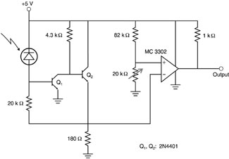
mode. A circuit that provides this mode is shown in
Fig. 17 (96) This circuit is capable of very high-speed response. It is possible to obtain rise times of one nanosecond or below with this type of circuit. (97) The biggest disadvantage of this circuit is the fact that the leakage current is relatively large, so that the shot noise is increased. (98) Many different types of circuits have been designed for photodetector operation for particular applications. We will present two specialized circuits for specific applications. These will give an idea of the range of circuits that may be employed for detection of radiant energy. (99) Figure 18 shows a circuit designed for detection of far-infrared radiation, in the 10-m m region. The detector is a mercury cadmium telluride detector operated in the photoconductive mode. This detector is a cryogenic detector, operated at a temperature of 77 K. It is generally packaged in a Dewar assembly and cooled with liquid nitrogen. The input radiation is chopped with a rotating mechanical chopper wheel, to provide an AC signal. This circuit has been designed for low-noise operation.
Fig. 18 (100) Figure 19 shows a circuit designed as a receiver for high-frequency fiber-optic communication systems. The circuit uses a back-biased silicon photodiode. It provides an output with transistor-transistor logic (TTL). In this system, the light emerging from the optical fiber is incident on the detector. The resulting signal is amplified. If this circuit is employed in a relay station in a telecommunications link, the output may be used to drive a laser diode source that retransmits the information into the next segment of the fiber-optic cable.
Fig. 19 (101) Now let us turn to the circuitry employed for photomultiplier tubes. In the circuits discussed above, the voltages were low, five volts to a few tens of volts. The photomultiplier tube requires higher voltages, in the kilovolt range. (102) Because the gain of photomultiplier tubes is a strong function of the applied voltage, a small change in power-supply voltage will result in a large change in gain. Thus, one must use a well-regulated, stable power supply for photomultiplier applications. (103) The power supply for a photomultiplier consists of a voltage-divider circuit, as illustrated in Figure 20 for a 10-stage photomultiplier. The total voltage around 875 V is applied from the anode to cathode. A string of resistors of equal value is connected in parallel with the dynodes. This ensures that the voltage applied from one dynode to the next is equal. This arrangement is called a voltage-divider network. It is the arrangement usually employed with photomultipliers, instead of applying separate voltage sources to each dynode. The circuit shown is a half-wave rectifier circuit. The connections are to the pins on the socket into which the photomultiplier tube is inserted.
Fig. 20 (104) An alternative arrangement is shown in Figure 21 for a 12-stage photomultiplier. This circuit uses a regulated DC power supply as the voltage source. The voltage-divider network is similar to that shown in the last figure. Although again the connections would be made directly to the socket pins, the connections are shown to the internal structure of the tube in order to make clear the functionality. The use of the adjustable resistor R1 is not strictly necessary. Its purpose is to minimize dispersion of the transit time of the electrons, but for many applications it could be eliminated from the circuit.
Fig. 21 (105) These two examples illustrate the general principles of power supplies for photomultiplier tubes. (106) For many of the diverse applications for which photodetectors are employed, the photodetector circuits are custom designed for the needs of the specific application. One exception, for which standardized packages are available, involves photodiodes for use in the visible and near infrared. Manufacturers offer integrated photodiode/preamplifier circuits. The photodiode is integrated on the same chip with an operational amplifier. Both photovoltaic-mode and photoconductive-mode chips are available. Thus the circuitry is already integrated with the detector and the user needs only to supply the specified voltage inputs. (107) Monolithic amplifier units specifically designed for use with photodetectors are also available. The amplifier converts the signal from a photodiode directly into a voltage that can be used to drive an oscilloscope, recorder, or other voltage-sensing equipment. (108) Most of this discussion about circuits has involved circuitry for photon detectors. We briefly describe some circuits for thermal detectors. Figure 22 shows the basic circuit for a thermal detector that employs a temperature-based change in resistance, such as a thermistor or bolometer. In this very simple circuit, the signal arises from the change in voltage drop across the load resistor when the resistance of the detector element is changed by heating by the incident radiant energy. If the load resistance is much smaller than the resistance of the detector element, the percentage change of the signal will be maximized.
Fig. 22 (109) Figure 23 shows a circuit for use with a pyroelectric detector and a pulsed source of light energy. The pyroelectric detector is a capacitor formed by depositing metal electrodes on a piece of pyroelectric material, such as lithium tantalate. The detector response arises from the change of electric polarization of the material with temperature. As radiant energy is absorbed and the temperature rises, the change in electric polarization leads to a displacement current in the material, which in turn causes a compensating current flow in the external circuit. The pyroelectric element in this mode acts directly as a current generator. The output signal is derived from the voltage drop across the load resistor.
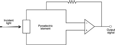
Fig. 23
Care and Handling of Detectors (110) The user must take appropriate precautions when handling and using optical detectors. These are delicate semiconductor devices that are subject to damage from a number of causes. (111) First, the recommended maximum voltage specified by the manufacturer should not be exceeded. Also, the current must be held below limits that would cause damage. For silicon photodiodes, this is about 10 milliamperes DC, or perhaps 100 milliamperes for short pulses. (112) Optical detectors are particularly vulnerable to damage by the high-power laser beams. Laser damage in detector materials is usually irreversible damage in the form of surface melting or vaporization. In some cases the electrical leads to the detector may become separated. A damaged detector may cease to function entirely, or may continue to operate with lowered responsivity. (113) Under easily attainable levels of laser irradiation, common optical detector materials may be permanently damaged. The laser irradiance striking an optical detector must be limited to ensure that it is below the damage threshold. (114) Photodetectors may be permanently damaged by excessive heating during soldering. The maximum soldering temperature and dwell time must be limited to avoid this damage. The use of a heat sink, such as a pliers, between the solder point and the detector element can be helpful. For silicon photodiodes, the maximum soldering temperature should be kept below 265° C. The solder time should be kept below 3 seconds for devices with plastic cases and below 7 seconds for devices with metal cases. (115) Excessive bending of the electrical leads or mechanical stress on the leads may cause failure. Forces used in bending, pulling, or twisting the electrical leads should be kept low. (116) Electrostatic discharge can damage photodetectors. Photodiodes are especially sensitive to damage by electrostatic discharge, although they are not as sensitive as laser diodes, as was discussed in Module 4-6. Photodiodes with high shunt resistance are particularly vulnerable to damage from this cause. Good control practices for eliminating static electricity should be employed when handling photodiodes and optical detectors in general.
Photodiode (Centronic OSD100-5T or equivalent) Operational amplifier (National Semiconductor LF356 or equivalent) Electric motor with toothed chopper wheel (Laser Precision CTX-534 Variable Speed Optical Chopper or equivalent) Helium-neon laser (few-milliwatt output) Resistors (selection of values, kilohms to megohms) Neutral-density filters (selection of different values, with total neutral density at least 4) Oscilloscope Power meter (Spectra-Physics Model 405 or equivalent) Argon ion laser (line tunable, with at least 4 visible wavelengths available) 
(117) In the first part of the procedures, you will fabricate a circuit to operate a photodiode as a photovoltaic detector and use it to measure the responsivity of the photodiode. (118) The experimental arrangement is shown in Figure 24. This uses the circuit for photovoltaic operation of the photodiode shown earlier in Figure 16. The toothed wheel is mounted on the electric motor. When the wheel rotates, it periodically blocks the light from the helium-neon laser from reaching the detector. The speed of the motor should be adjusted so that the light is blocked 1000 times per second. This is a standard measurement condition. If the wheel has 10 teeth, for example, the motor should rotate at 100 revolutions per second.
Fig. 24 (119) Hook up the circuit as shown in the figure. The load resistor should be much smaller than the value of the shunt resistance of the photodiode, which is specified by the manufacturer. Feed the output of the circuit into the input of the oscilloscope. (120) The output on the oscilloscope screen should be a 1000-Hz square wave. Use the voltage calibration of the oscilloscope to measure the peak voltage of the signal. Then insert the power meter into the laser beam in front of the photodiode and measure the power in the beam. Calculate the responsivity of the detector and compare it to the manufacturer’s specification. (121) Next, check the linearity of the detector response by inserting neutral-density filters into the path of the beam as indicated. Gradually increase the number of neutral-density filters and record the total neutral density and the peak voltage at each step. Increase the neutral density to at least 4, increasing the sensitivity of the oscilloscope display as necessary. Plot the peak voltage as a function of neutral density on semilogarithmic paper. The plot should be a straight line. (122) Next, you will operate the photodiode in the photoconductive mode. The experimental arrangement is shown in Figure 25. This uses the same circuit that was shown in Figure 17 for operation of a photodiode in the photoconductive mode.
Fig. 25
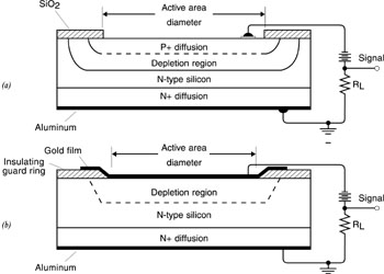
(123) Hook up the circuit as shown in the figure. The load resistor should be relatively large, in the megohm regime. Feed the output of the circuit into the input of the oscilloscope. (124) The output on the oscilloscope screen should be a 1000-Hz square wave. Use the voltage calibration of the oscilloscope to measure the peak voltage of the signal. Then insert the power meter into the laser beam in front of the photodiode and measure the power in the beam. Calculate the responsivity of the detector and compare it to the manufacturer’s specification. (125) Next, remove the power meter and change the value of the load resistor. Use several different values of load resistor and for each one record the value of the peak signal. Plot the peak signal as a function of the value of the load resistor. How does the signal vary with load resistance? (126) Now you will measure the responsivity as a function of wavelength. One measurement is already available, at 633 nm. Use the line-tunable argon laser to obtain values for at least four different visible wavelengths. (127) Replace the helium-neon laser in Figure 25 with the argon laser. Replace the load resistor with the same value that was used for the responsivity measurement at 633 nm. For each of four different argon laser wavelengths, measure the peak voltage on the oscilloscope and the laser power reading with the power meter in the same way that you measured them at 633 nm. If the argon laser power is too high, insert neutral-density filters in front of the photodiode and the power meter to reduce it to an appropriate value. Record the results and calculate the responsivity for each wavelength. Plot the responsivity as a function of wavelength and compare the result to the manufacturer’s specification.
Photovoltaic mode measurements Peak voltage: _________ Power meter reading: _________ Linearity measurements. Total neutral density Peak voltage 1. 2. 3. 4. 5. 6. 7. 8. 9. 10.
Photoconductive mode measurements Peak voltage: _________ Power meter reading: _________ Measurements of effect of change of load resistor Load resistor Peak voltage 1. 2. 3. 4. 5. 6. 7. 8. 9. 10.
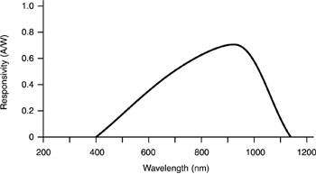
Measurements of responsivity as a function of wavelength
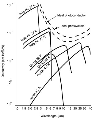
1. 633 2. 3. 4. 5. 
1. Define detector responsivity, noise equivalent power, quantum efficiency, detectivity, and rise time. 2. Define sources of detector noise, including shot noise, Johnson noise, 1/f noise, and photon noise. Explain methods employed to reduce these noise sources in the detection of optical radiation. 3. Describe and explain important types of photodetectors, including photon detectors, thermal detectors, photoemissive detectors, photoconductive detectors, photovoltaic detectors, and photomultiplier detectors. Describe the spectral response of each type. 4. Draw and explain circuitry used with photomultiplier detectors. 5. Draw and explain photodiode circuits for use in the photoconductive and photovoltaic modes of operation.
Dereniak, E. L., and D. G. Crowe. Optical Radiation Detectors. New York: Wiley, 1984. Jacobs, S. F. "Nonimaging Detectors." Handbook of Optics, W. G. Driscoll, ed. New York: McGraw-Hill, 1978. Kruse, P. W., L. D. McGlauchlin, and R. B. McQuistan. Elements of Infrared Technology. New York: Wiley, 1962. Chapters 8-10. Photomultiplier Handbook. Lancaster, PA: Burle Industries, 1980. Vincent, J. D. Fundamentals of Infrared Detector Operation and Testing. New York: Wiley, 1990. Yariv, A. Introduction to Optical Electronics. New York: Holt, Rinehart and Winston, 1976. Chapter 11.
|

 Equation 4