Digital PC Oscilloscope

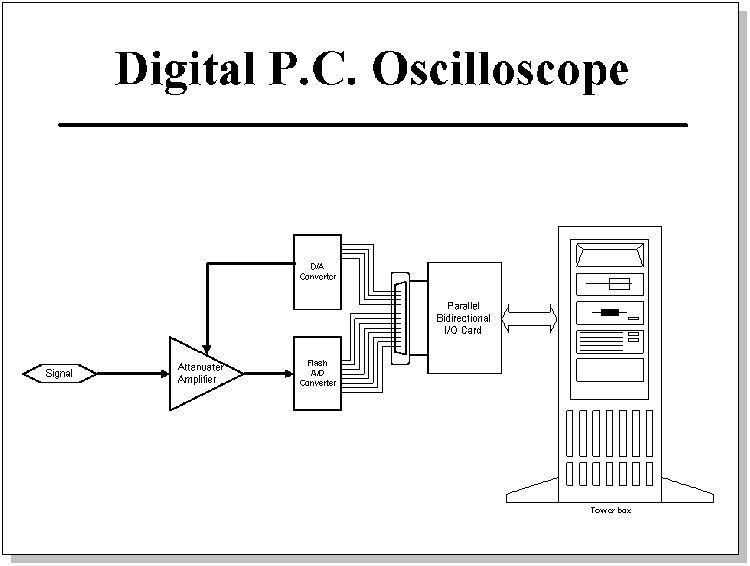
Overall Block Diagram (click here)
Our group decided to pick the Personal Computer Oscilloscope because it sounded very interesting to approach. We also felt it would help us in understanding many aspects of hardware and software interfacing. We also wanted to do something that we felt was consumer electronic related to the current market and was interesting in working with.
This particular digital pc oscilloscope that we produced was successful in running, although it did not meet all of our hopes and goals stated in the proposal.
Briefly, the system contained many stages of operations necessary in a successful model. First of all, the system contained an external circuit layout that was used to do the Analog to Digital converting, the Digital to Analog scaling, the clocking, and the aliasing detection. The other stages are internal to the computer, such as; the I/O card interface, and the Visual Basic programming which displayed the data.
In this write up we will be describing all the necessary components and how they are implemented into the system functions. We will also be describing the system software and the necessary program that allows the computer to interface with the external circuit.
Finally, we will give a description of the background information we received from a local company, stating the current marketing digital oscilloscope that operates on the personal computer.
When we started working on the personal computer oscilloscope we first needed an excellent A/D converter. The first one we tried was a complete mistake. The problem with this integrating converter was that its sampling frequency was really slow (4Hz), which only allowed us to look at frequencies under 2Hz, and even those waveforms were ugly. Then we decided to put in a really fast 250Mhz, but we could not get that converter to work. The 250Mhz converter was very difficult to work with, for it required a lot of precision biasing. So, we installed the final converter (70kHz) which isn't the greatest converter, yet it was easier to work with and sampled at a high enough rate for this particular project.
While working on the proper A/D converter, we began the computer interfacing process. This process required a good I/O card and Visual Basic programming to read the card. This process was ever building in the project designing, we simply kept including extras in the program for ease in operating. The I/O card was easy to decide on because it provided us with the ability to upgrade and it was programmable for; read, write, or bi-directional. Also, the I/O card had the necessary amount of bit locations to be used in our bi-directional interface programming.
One problem that we found with this system was that we could only input data with maximum voltage of 3V, otherwise the A/D chip would burn up. So, in order to save the chip we put in 2.7V zener clipping diodes and built a D/A conditioner. This D/A stage circuit divides the voltage down immediately from the input signal, runs it through the A/D converter, which sends it to the computer. The program then realizes how much it needs to scale the signal such that the A/D converter gives the best resolution.
And the last thing we did was the aliasing detection circuit. This circuit's purpose was to recognize that the input frequency was to large for the sampling rate. Once this system recognized aliasing, it would send a high signal to the port and the window would display ALIAS on the graph. The circuit consisted of a frequency to DC voltage converter and a comparator.
The system was surprisingly cooperative and we ran into little complications, which allowed us to have a successful working model, and a system that basically simulates the market pc oscilloscope.
To display analog signal onto a digital computer, such as your PC, the continuous analog voltage needs to be converted into a discrete digital number that the computer can then take and manipulate. The conversion between analog to digital is done using an A/D converter chip. The fact that we are changing continuous signal into discrete implies that the faster of an A/D converter we have, the better we will represent the continuous analog signal into discrete digital as well as the fact that we will be able to accurately reproduce higher frequency waves. Today, two methods in A/D technologies seem to give the best speed performance.
One, is sequential approximation, in which the analog voltage is approximated by sequentially moving from the most significant bit to least significant bit and comparing the digital voltage to the analog voltage. The method works similarly to a binary search in which we do a binary search for the digital number that best represents the analog voltage. One drawback to this method is the fact that the chip must also contain a digital to analog stage to transform the digital voltage into analog and compare it with the analog input.
The second, and by far the most popular method for use in high speed electronics, is a flash A/D converter. Suppose that one uses an 8 bit converter. Then, 256 (2^8) comparators are stacked one on top of each other and the input voltage is passed through a 256 resistor network ladder. Without going into too much detail, the resistor network will distribute the input voltage evenly on each resistor and the comparators compare each node signal against a fixed reference voltage. Based on how many comparators are "on" at one time, a digital number representing the input voltage can be obtained.
In our design, we decided to use Motorola's triple 8-Bit Video ADC (MC44250).
This flash A/D converter has the following feature which made it extremely well suited for our project:
If one is to use the chip at its full speed then the ground layer should be separated into an analog and a digital ground, with enough space in between them to minimize coupling (in the above drawing the triangle represents analog ground, while the 3 line triangle represents digital ground). When running at speeds around 70KHz we did not find it necessary to worry about coupling. We were able to get away with using the same power supply and same ground for both the analog and digital part of our design. Each power supply pin should be decoupled to ground as close to the package as possible (see reference 1).
Depending on the environment in which the circuit is being built, a large coupling capacitors might be necessary in order to remove any excessive noise around the components (one environment in which this applies is when the circuit is built using a breadboard).
R1 is used for current biasing, and 5.1K is recommended for optimal performance.
Our A/D converter requires a clock running at speeds up to 15MHz. In our project our speed was not limited by the external hardware, but rather by the programming language we decided to use. Hence, using a very high speed clock would not have been of much help. Instead, for our clock we used the basic astable circuit described below (see reference 2). With R1 equal R2 and C1 = 0.01u we obtained extremely good (50 % duty cycle) square waves in the range of about 100KHz.
Again, caution should be taken on where and how the clock is mounted in the circuit. On a breadboard, the high clock frequencies will cause excessive noise causing certain components to malfunction. In our setup we had to mount the clock on a circuit away from the breadboard.
We decided that it would be nice to have the ability to measure a 100V peak to peak wave. However the D/A converter is rated for only 25V. By using the 3K and 1K resistors we made sure that we have a 25V input to the DAC when the original wave is 100V. The rest of the circuit acts just like an inverting amlifier where we are using the DAC as the feedback voltage. Using this setup we are able to divide the input signal by a factor ranging from 4 to 1024. (By the fact that we always divide the input signal one must realize that this is not the optimal configuration for a scalar. Ideally one would like the scalar to have the ability to both amplify and attenuate the input signal)
Our A/D converter requires the input voltage for Vin to range from around 1.7 volts to about 4.9 volts, with an average range of about 3 volts. Moreover, since the A/D data specs did not contain any information on the input impedance it would be nice to have something that would provide high impedance to the analog input as well as shift the voltage in the +2V to +5V range.
The below circuit provides us with exactly what we need. The two zener diodes will clamp the input voltage to plus or minus 3.4V (0.7 + 2.7). Adjusting the gain on the amplifier, via R2, we can obtain a translation in the range +2.5V, -2.5V to a range of +2.0V, +5.0V. with no input wave distortion.
When sampling continuous signals caution should be taken to prevent aliasing. By definition alias is a false signal caused from beats between signal frequency and sampling frequency (see Window Display for Oscilloscope(below) : in this picture a very high frequency sine wave is sampled at a frequency lower than 1/2 its own and we see something that is perceived to be a slower frequency sine wave). In 1928 Nyquist discovered that in order to prevent aliasing the signal must be sampled at a frequency twice its own. Hence, we thought that it is only appropriate to incorporate an alias detection circuit in our PC Oscilloscope.
Click here for Window Display for Oscilloscope
The circuit below converts frequency to voltage and then using the LM339 comparator we compare this voltage with a preset voltage adjusted by R13. The voltage at R13 is adjusted to be equal to the voltage from the frequency to voltage stage when the input frequency is at the aliasing point. The comparator will be low when we are operating in the good frequency range, and high when we are aliasing.
The Visual Basic program must accomplish the following tasks:
The first three tasks are tightly binded together and the correlation between them can be described by the following flow chart.
Click here for Flow Chart
Click here for Visual Basic Program
The program works as follows. Originally the attenuator divides the input
signal by 256. If our input is a large voltage then the A/D converter will be
able to display a clean wave, and the program follows path "a". However, if
the input signal was small to begin with, then the A/D converter will not be
able to read a correct representation of the input signal. We will then see a
mere "0". The program will then find the maximum number coming from the A/D.
This number will be much smaller than our threshold value and number 2 from the
decision box turns out true. Therefore the program will tell the hardware to
divide the input by a number twice as small as by what we were previously
attenuating, and the program follows path "b" until the decision box turns 1 to
be true and the program changes to path "a".
Now suppose the we are at a nice voltage, we see a clean wave on the scope and everything is adjusted just right (we are following path "a") when all of a sudden the input voltage either drops or increases dramatically. How will the program behave?
Well, let's take each case one at a time. If the voltage drops bellow the threshold voltage then the collected digital data will have a number below the threshold number and the decision box turns number 2 as true and we will follow path "b" until the collected digital data is above the threshold number. Once that happens the program switches back to running path "a".
Next, if the program is going along path "a" and all of a sudden a high voltage comes at the input, the D/A converter will read a number very close to FF-hex (please note that the D/A converter will not damage because of the zener diodes on the analog to digital conditioning stage). The number read by the A/D converter will be larger than the ceiling number and the decision box will turn out number 3 as true. The program tells the attenuator to attenuate to the maximum (we are now following path "c"). As soon as this happens the next stage the program will follow path "b" (can you tell why?).
If we were to watch the program for a while one would note that path "a" is the equilibrium path. Anything that happens our software will try to bring the state of the machine in the state described by path "a".
The A/D converter will always give a number between FF and 00 with 7F at equal distance between the two. Anything above 7F is positive and below 7F is negative.
By taking the absolute value we can deal only with the positive part. We divide the upper range as in the following picture
Our ADC will give the best resolution when the amplitude of the signal is between 2 and 4. (See software program on how this is solved scope55() and scal() are the functions doing this)
The idea behind triggering is best explained by the following picture:
Because the time to sample the digital data and the time to display it are not equal we need to add a time delay to synchronize the graphed, otherwise the graphed data will be jumping around the screen as the screen is updated.
Marketing Personal Computer Digital Oscilloscopes
Rapid Systems, Incorporated
R2 Universal Digital Oscilloscopes
A very interesting aspect of this project was talking with engineers that build these PC oscilloscopes for actual consumers. One particular place we were able to talk with was Rapid Systems. Rapid Systems was very helpful in answering all of our questions. They even provided us with a manual on the three systems, Analog to Digital Converter Chip names, and a demo disk pertaining to the actual operating window.
When talking with Rapid System we learned that their system was quite similar in block diagram layout that we designed. Due to lack of necessary time and money we were unable to meet the specifications that the marketing PC oscilloscope are running at.
The three PC oscilloscopes that Rapid Systems provides for the consumer are:
These three oscilloscopes all use C assembler for programming the I/O port described in the details. They also use Matrix Layout as the software program that allows them to design a well detailed window for viewing purposes.
Noticing the abilities of these three well thought out oscilloscopes for the PC, we now can determine what to do differently in the future. For one thing, we would like to use an I/O card that samples in the MHz range (Rapid Systems developed their own I/O card). We felt our major set back, was the Visual Basic software we used to program the I/O card and viewing window. Visual Basic is really excellent in monitoring systems or running visual programs at lower sample rates, but is absolutely terrible in running sample rates in the KHz range. The limitations of the two (interface card and software) were the main contributors to the 500Hz maximum sampling rate. Although, we were able to observe very interesting aliasing wave forms over the 500Hz range.
Although we obtained detailed information regarding material used on marketing oscilloscopes, we were unable to convince them of giving out design information. This information would have been extremely helpful in answering the more specific questions, regarding the circuit design and software interfacing. One way of us obtaining this information would be to go out and purchase one of these systems, taking it apart and analyzing it.