Assembly and Construction
As a reference you may wish to print out the page containing the circuit diagram or open up a
new window.
ASSEMBLY
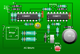
A small perforated board was used approx. 2 ½" by 1¾". Components were layed out as per the diagram below. For ease of wiring, and good practical design, sockets are used for the two 14 pins IC's .
Use a slightly larger board to start your work. Study the lay-out and notice that some of the tracing connecting the pins of each IC are in black and others in blue. The blue tracing should be on the components side but you can reverse the connections if you wish . On the face of the board mark the areas where the two IC's are to be located as well as the number of each IC pin to be connected by jumper- wire, marked in black on the lay-out. This can easily be done by inserting small wire size #26 or smaller into each pin holes before inserting the sockets .
Double check your jumpers insertion then gently press the sockets into the holes firmly on top of the jumpers . If you cannot insert the sockets on top of the jumpers enlarge the holes until you can fit the sockets. When this is accomplished , use a testmeter and check that connections are good on the socket connectors. Then turn the board over and solder the pins with the jumper wire connections. Check and double check before soldering -- one mistake and you may have to rip the socket out and redo the set-up with a new socket .
On the wiring side of the board solder the two jumper wiring connections under the CD4001 as indicated in blue on the lay-out. Now you are ready to assemble all the components as they appear on the lay-out. Resistors lead wires should be formed to fit the four holes distance except for R7 which occupies more space. Capacitors and diodes use three holes. Feel free to modifiy as required .
R7 values required for proper voltage drop and zener current limit is 16.8K/ 2W. I subsituted two resistors on hand each of 33k/1W connected in parrallel. These large resistors should be installed away from the board as they will dissipate some heat.
For the rectifier bridge I used four rectifier diodes (1N4005) from my junk box. But you may use a rectifier brige module of equivalent specifications if you wish . Before installing the SCR make sure you have enought room for R9 , which incidentally may not be required after testing and substituted with a jumper connection to the gate .
Make sure that all the diodes are properly oriented with the end band being positive and laid out as shown.
As you can see on the lay-out most connections are made with the component leads cut at the connection points except for the positive and negative busses which can be made with a bare wire #20 from point to point. Holes must be made larger for connecting the AC wires at the bridge and SCR connections .
DO NOT INSTALL THE IC'S UNTIL A COMPLETE VOLTAGE CHECK
IS DONE
TESTING
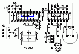
Satisfied that the board has been checked for errors, use a 9 volt source connected at the negative end of C4 and the positive at the junction of D8 and ZD1. Check for proper voltage minus the diode voltage drop ( .5V) at pin #14 of each IC 's socket. If ok then disconnect the power source and install the ICs.
Then using 3 to 4 inches of wire make connections to the R11 potentiometer. With the shaft toward you, the wiper left connection is made to point A (D1)and the right to point B (D2). The center connection is made to points C (jumper R2 and R3). Then reconnect the power supply and with a scope connected from ground (neg.) to TP1 you should see a slow oscillation that you can vary with the rotation of R11. If no scope is available a voltmeter can be used to monitor a voltage deflection from zero to about 4.5 volts. In either case this is an indicatation that CD4001 is functioning properly.
Until all connections are completed this is all we can test for.
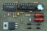
This the size of the prototype actual size