Function Generator
I was having some problem with my function generator that I build over ten years ago with an ICL8038 chip and was having problem with the output voltage calibration and the DC level output setting.
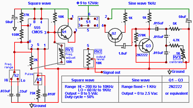
Rather then dig into the circuit to find the problem and since I did not need all the trimmings I decided to scrap it and design a more simple and reliable system using the 555 Timer IC for the square wave and discrete components for the sine wave .
The system consists of two seperate circuits , while the square wave genator is variable from 60 Hz to 10KHz the sine wave is limited to a fixed 1Kz. The two circuits can be combined with the use of S1 or used separately .
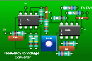
In addition to the generators another circuit is used as a Frequency to Voltage converter using the LM331 IC . This cicuit will enable you to read the frequency output with a digital voltmeter .
Square wave
The output is a 50% duty cycle , the range is selected with S2 and the frequency is adjusted with RV1. S3 has been added to change the square wave to a sharp pulse by shorting the .01uF from pin 5 to ground with the 75K resistor , this value appeared to be just right for the pulse but it can be adjusted by choice while observing the pulse width output on an oscilloscope.
The frequencies specified are approximate and depend on the components used especially the timing capacitors .033uF and
and .33uF which are soldered directly to S2.
S1,S2,S3,RV1and RV2 are the external controls while RV3 is a miniature potentiometer installed on the circuit board for a limited range of calibration of the 1Khz sine wave output , I used a ten turns trimming pot for RV3. The signal output is taken from either Q1 or Q2 emitter which are wired as output voltage followers/buffers for low impedance output and connected to the output level control RV1 . Please note that Q1 and Q2 must have a constant emitter load, in this case the 10K ohms of RV2
for an undistorted wave, a lower 5K pot can be used but will only result with an increase in current consumption . A fixed load resistor instead of RV1 will result in a full signal output level from the emitter output .
As mentionned earlier the circuits are individually selected with S1 for either a Square or Sine wave . Notice that the power supply is also switched, this to prevent any possible cross signal interference .
Sine Wave
The sine wave circuit is a twin "T" oscillator. The frequency is the pruduct of the tree .015uF capacitors with the 5K ,4.7K and RV3
of the twin "T" circuit . Other frequencies can easily be obtained by changing other capacitors of equal values and /or resistances
experimentally but with a limited adjustment range for a good sine wave output .
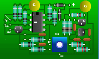
Generator Layout and PCB
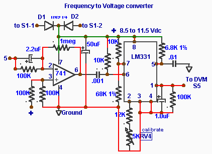
Frequency to Voltage Converter
I include this V to F converter circuit with the LM331 chip, if you already have a frequency counter needless to say you may not have a use for it but for those who have not , you may still be able to find the LM331 even though it has been out of production since 1995.
The data sheet specifies a linear accuracy of .06% up to 10Khz with the standard suggested circuit shown below minus the conditioning circuit made up of the 741 which I designed to condition both the square and sine wave to be acceptable to
the LM331 input . Actually combined with my DVM error the best I ever could obtain was 1 to 1.5% linearity .
The input is taken from S1-5 or directly from the transistor emitter output and the F to V output voltage fed directly into the DVM 2Vdc range input for up to 1.999 Khz to read one milivolt per Hz or to the next higher range of 20Vdc for the maximum 10Khz or 10Vdc .
Diodes D1 and D2 connect the power supply from S1-1 and S1-2 and permit supply voltage to the converter when either one of the generator is selected without back feeding voltage to the OFF generator, thus a half volt drop through the selected diode is the result .
The diodes are not needed if only one generator is to be used . The diodes can also be removed if a 3PDT is used for S1.
To obtain this maximum reading of 10 V a supply of 12v is required .
The V to F converter would be a welcome addition combined with a DVM module which could be mounted on the front of the
enclosing cabinet , the price of such DVM module can be had for less than U.S. $20.00.
Calibration of the converter is done with on board trimmer RV4 preferably a small 10 turns trimmer and would require access to a frequency counter for accurate setting but short of that a low voltage transformer with output connected to a rectifier diode and series resistor would provide a signal for a 60Hz calibration . Any other known source of frequency within the specified range like the calibration square wave output of an oscilloscope could also be used .
F to V Layout and PCB