Assuming you have acquired or have access to the most basic of construction equipment:
(a) a small tip soldering iron - about 15 watt
(b) some small gauge resin cored solder
(c) a pair of diagonal cutters
(d) a pair of small pointy nose pliers
(d) and a multimeter - preferably digital
and you have some basic soldering skills or you can practice on some scraps you can now proceed to constructing the most valuable piece of test equipment you will probably ever construct.
If aren't familiar with basic electronic terms and schematics and you haven't read these tutorials THEN DO SO NOW:
3. Radio Basics
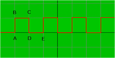
Firstly let's look at Fig 1. which is meant to represent a snapshot of a square wave signal as it might be seen on a simulated oscilloscope.
Now over the green background of our simulated oscilloscope (hereafter called a CRO - short for Cathode Ray Oscilloscope) you can see black / grey horizontal and vertical graduations. They represent the horizontal time base settings and the vertical amplifier settings. In Fig 1 we have set our vertical amplifier to represent 5V per division and the horizontal timebase setting to represent 100 micro-seconds (100 us).
As you can clearly see from this simulated signal it's value goes from zero volts (the centre horizontal line - at point A) up vertically to the next horizontal line (representing 5 volts - at point B). The signal continues horizontally for one graduation to point C before returning to zero volts at point D. Our signal continues horizontally for another graduation at zero volts to point E.
The total period of time our signal takes to complete one full cycle (Points A through to E) is two graduations of the horizontal scale, each of which represent 100 us, total time is 2 X 100 us.
Frequency = 1 / time which is 1 / 200 us OR
Now I've gone a long winded way about describing for you what a square wave signal (this one at 5 Khz) looks like. It is generated by a "multivibrator".
O.K. get to the point - what's a multivibrator? It is simply an electronic device which simply turns on and off at a pre-determined rate, in this case 5 Khz or 5,000 times a second.
A lot. A unique feature of square wave signals is that they are "RICH" in what we call "harmonics". You not only get 5 Khz, you also get 10, 15, 20, 25 ........450, 455, 460 Khz etc. forever etc. until the signal becomes too weak.
Now here is the beauty of the device, if we build a multivibrator running at say around 2 Khz we're going to get those rich harmonics all the way up into the r.f. region. If we are trouble shooting an audio amplifier we have harmonics at 2 Khz. 4, 6, 8 etc. which our audio amplifier can easily reproduce. If we are trouble shooting an i.f. amplifier at 455 Khz then I would expect the harmonics to still be quite stong enough to be heard up there as well as being quite usable much higher in frequency.
It's cheap to construct, it's relatively easy to construct - with some practice for some novices and, it's a pretty versatile tool to own.
Here it is in fig 2.
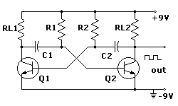
Firstly you will notice it is powered by 9V which of course can easily be provided by a convenient size battery (so it's portable). There are only two general purpose NPN silicon transistors used (types to consider 2N2222A, BC107 - nothing sacred here just any convenient NPN silicon you can easily and cheaply get hold of). Find out for absolutely certain the pin outs! That is which are EBC. It needs a gain (Hfe) of at least 120 with these values - see addendum later.
This circuit consists of two cross coupled amplifiers comprising Q1 and Q2 ( NOTE: where the diagonal lines cross over in the schematic in fig 2 (and later fig 4) there is NO connection.
REPEAT AFTER ME: "where the diagonal lines cross over in the schematic in fig 2 (and later fig 4) there is NO connection".
Neither of these transistors are EXACTLY identical so when we switch on, one of them is going to take control first. Let us assume this is Q1. It will turn on hard (just like a light switch) but C1 will now begin to charge up through R1 (timing is R1C1) and because the base of Q2 is connected to this point it will rise toward the 9V with the same timing. At about 600 mV Q2 will start to conduct (switch on) and the voltage at the point of connection between the collector of Q2, C2 and RL2 will begin to drop.
Because this decrease in voltage is coupled back to the base of Q1 through C2 so Q1 begins to switch off with Q2 now switching on even harder but C2 will now begin to charge up through R2 (timing is R2C2)and the whole process just repeats itself over and over. All the while the voltage at the collector of Q2 switches from about 9V (when Q2 is OFF) to 0V (when Q2 is ON) - BTW in case you're wondering, the 9V disappears as a voltage drop across RL2. Now in the real world you won't get a switching action of exactly between 0 and 9 volts AND it won't be an exact square wave as depicted in fig 1. What you will get is a rough approximation to suit our end purposes, i.e. an harmonic generator to use for trouble shooting.
Now for the purists I could have given a more detailed and scientific explanation BUT is that what we're on about here with this beginner (and even not so beginner) electronic project?
The ON / OFF period (called "mark/space" ratio for the purists) - look back at fig 1 that's what it's for, is determined by R1C1 and R2C2. If we make R1 = R2 and C1 = C2 it can be shown mathematically, (and I won't bore you) that Fo = 0.7 / (R * C).
Using this formula and assuming we have a resistor value of 39K for R and a capacitor value of 0.01 uF (same as 10 NF) we get a frequency of approximately:
0.7 / [ 10 X 10-9 X 39 X 10+3]
Using my calculator I get an answer of:
0.7 / 0.00039 = 1795 Hz
Did you get that answer? NO? If not, why not?
In case your confused we are using the exp function on your calculator. 10 X 10-9 means I entered 10, then hit exp, then entered 9, then hit the +/- key (not the subtract key). Do the same for the 39 X 10+3 figures (having hit the "X" or multiply button first) but this time not using the +/- key. I put that "sum" in memory with M+ then enter .7 and divide with RM (recall memory). Your milage might vary with the calculator you use. Learn how to use it!
Now 1795 Hz is ideal for our purposes. NO it doesn't have to be exactly 2,000 Hz or 2 Khz.
Here's the real "icky" part and it depends on what you can scrounge. Even if you puchased the above parts new you should not have spent $1. What we do next depends entirely on how you want to package your square wave signal generator.
As it is going to be a "service" tool we want to house it in someting hand held. If you can't buy anything else suitable, consider scrounging a piece of PVC plumbing tube or even electrical conduit, say about 1 1/4" (32mm) diameter (must be able to accomodate 9V battery with snap attached), cut to a suitable length of about 4" (100 mm). These dimensions are not sacred (from memory my original one was 2" - 50 mm tube) as long as we have space for the battery, our circuit board and, these other components AND it's comfortable in your hand.
To this we are going to add a probe sharpened to a point at one end. Also we are going to add a red led (light emitting diode) and a push button switch. See figure 3
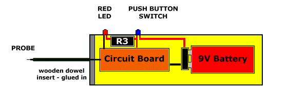
From this diagram you can see we have a piece of PVC tube which will conveniently house a 9V battery with it's battery snap (clip) attached. We will have a piece of Vero or perf board suitably sized to fit. Also we have glued in our red led (after drilling a suitable size hole) and similarly we have fitted our push button switch. This probe we might have made from a discarded screwdriver which has had the head damaged but we have now ground it down to a pointy end and preferably covered with some sort of insulation such as heat-shrink tubing, that is except for the pointy tip.
Hey! - y'all have to improvise here folks.
Now the whole idea of this is we have a giant "Biro" or ballpoint pen which fits comfortably in our hand, allows us to use our forefinger to press the push button and "believe it or not", on mine, the red led provided some illumination in the deep recesses of radios.
Also with mine (the original one that's gone to the sky) I got cunning and found if I used a hole saw and drilled a hole in some scrap material slightly larger in diameter than the inner diameter of the PVC tube I had a neat end plug to glue into the PVC tube to house the old screwdriver. I actually used 1" thick scrap timber as I found this gave me some rigidity in holding the probe.
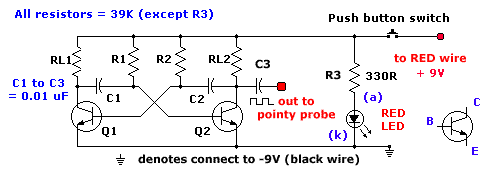
From this you can see where the black and red leads from the battery snap connect to. Doesn't matter which way your 0.01 uF capacitors connect (buy cheap 0.1" lead spacing types) nor do the resistor connections matter.
Resistor colour codes:
39K - if 4 colours - has Orange|White|Orange|Gold = 39K 5%
39K - if 5 colours - has Orange|White|Black|Orange|Red = 39K 2%
330R - if 4 colours - has Orange|Orange|Black|Gold = 330R 5%
330R - if 5 colours - has Orange|Orange|Black|Black|Red = 330R 2% ???? Check!
Check your resistor values with your multimeter.
The pushbutton should be a "normally off" type meaning it ONLY connects when you push the button.
Now the transistors and the led, the second hardest part. If you don't know the leads for certain, then wherever you buy these components from, have the sales clerk identify the leads for you. The transistors have an emitter (E), base (B) and a collector (C). The led has a cathode (k) and an anode (a).
Connections are shown on the final schematic. If you can't have the leads identified from where you purchase - DON'T BUY THEM.
6th January, 2001 - NOTES BASED ON FEEDBACK TO DATE: The values for your multivibrator square wave signal generator depend upon the gains on your individual NPN transistors, in some cases it may be beneficial to raise the values of RL1 and RL2 because your NPN silicon transistor gain (Hfe) needs to be greater than R1 / RL1. Using 330R for RL1 means your transistor gain should be > 39,000 / 330 = >118
If you experience problems then make RL1 = RL2 = >750 ohms, surely any decent transistor has a gain of better than 50.
You can use near values for your other resistors and the capacitors. The capacitors are standard 0.01 uF, I'd prefer a polyester or plastic type rather than ceramic. They are NOT electrolytic types.
Make SURE you wire it EXACTLY in accordance with the schematic in figure 4, use a multimeter to double check your wiring and to ensure NO shorts, that you have continuity where you should etc. The resistors and capacitors can go either way, the ONLY critical point is you correctly identify base, emitter and collector on your transistors. It is a pretty basic circuit.
These following points MUST all connect together - follow it on the schematic - and can be checked with a multimeter:
RL1, R1, R2, RL2, R3, SWITCH
RL1, C1, Q1(c)
R1, C1, Q2(b)
R2, C2, Q1(b)
RL2, C2, Q2(c), C3
Q1(e), Q2(e), LED(k), NEGATIVE OF BATTERY
SWITCH, POSITIVE OF BATTERY
R3, LED(a)
Using your multimeter, if you find connections beyond those listed above then you have made a mistake e.g. R1, CI DO NOT CONNECT TO R2, C2 - test it out.
Here you really have to improvise (again)
You have a choice of:-
(1) Printed Circuit Board - (2) Strip Board or Vero Board OR (3) Ugly style
1. Printed circuit board - this is fine if you are capable of fabricating a suitable board to fit in the available space. I suspect most readers will not have the facilities and I'm certainly not in the PCB production business.
2. Strip Board or Vero type Circuit Board - I suggest Vero or "strip board" if you can buy it. Cut it with a hacksaw or similar (gently) so it will cleanly fit into your PVC tube. This type of board looks like fig 5. The tracks with pre-drilled holes are parallel lines of copper track. Sometimes it is pre-tinned (depicted), sometimes not.
I have only shown the bottom view. NOTE: Components are normally mounted on the top side. Tracks and holes all follow a standard 0.1" (2.54 mm) spacing (called pitch). Adjacent tracks are insulated from one another and when one track needs it's continuity broken I use a 1/8" (3 mm) twist drill bit to enlarge the hole on the track side. Just use the twist drill bit in your hand and gently twirl the bit. A few turns of the twist drill bit and the copper track is broken.
To give you some general idea I have depicted two resistors mounted on the board. As I said before components are normally mounted on the top side but for clarity purposes only I have drawn them on the bottom. BTW sometimes it is necessary for space reasons to mount them on the bottom - there is NO sacred rule, just as long as it works.
This diagram relates to nothing in our project. It is simply to give you some idea of a vero type board layout.
Ideally before starting a project using this type of board you should try a few layouts on paper. Print out and use this strip board layout sheet as a guide.
You will notice the first resistor runs vertically down from track 1 to track 3. Each end of the resistor is insulated from the other. With the second resistor you will notice it runs horizontally along the track where the yellow circle underneath it is meant to depict that I have cut the track with my twist drill. Here again both ends have now been insulated from one another.
When using this method always constantly refer to both your circuit diagram and your layout sheet. Also always check for continuity [or where applicable, dis-continuity] with your multimeter.
3. Ugly Style - My old favourite. Doesn't look terribly flash but it's very practical. If you have ever seen underneath the chassis of an old valve receiver you will know what I mean. For a small project like this miniaturisation can be a problem requiring some ingenuity to overcome the difficulties. Firstly I'd try and locate some scrap PCB (printed circuit board) and cut it to suitable dimensions with a hacksaw to fit the project. If you can't get PCB then consider some thin scrap copper flashing (see your friendly plumber and do ask nicely) or perhaps thin brass sheet. I wouldn't consider any other material unless you are experienced. Most hobby electronic stores stock the materials I have spoken of here.
I would use the copper side of the PCB as a "ground plane" i.e. every component which needs grounding, including the black lead from the 9V battery snap connects here.
As one example:
You have your PCB cut to dimension - Looking at the schematic diagram in fig 4 we can to the left of the PCB solder the emitter lead of Q1 to the board by making a small right angle bend in that lead near the end. Now our Q1 transistor is nearly self supporting on the board (in a mechanical sense). Next I would trim the leads of RL1 and solder one end to the collector of Q1 (which in itself might need trimming).
Noting that R3 and the led can be mounted off the board we could perhaps consider soldering Q2 somewhere to the right of Q1 by also soldering it's emitter to the PCB. Next I would perhaps solder C1 between the junction of R1 and the collector of Q1 then across to the base of Q2.
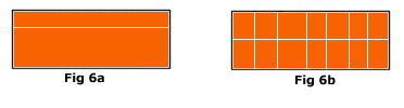
You could also consider this little trick to use. Why not cut a line lengthwise along your board with a hacksaw just deep enough to separate the copper? see Fig 6a below. In this way you can mount most components on the bottom section and the components which need connecting to +9V (red lead - after the switch - and it's called the "hot side") could be mounted on the top section. Or fancier still, why not cut the board into islands (called "pads") with hacksaw cuts see Fig 6b. You should have the general idea now.
You should have some hook up wire, just small gauge stuff to connect between the battery snap, the switch, the led, the PCB and finally the probe.
Next you need some foam rubber (thin stuff) to use as packing (hey we don't want everything floating around in the tube). By packing with foam rubber (gently) we ensure a neat fit eh!
Now go back and check ALL your wiring against the schematic. You just did that? GOOD!
Now go back once again and check ALL your wiring against the schematic.
Think I'm being paranoid? Want to know how many mistakes of my own I've picked up double and treble checking? PLENTY! Never apply power without double / triple checking.
Assuming you are both happy and confident (I'll bet), push the on / off button - the LED should light. Now turn on any old AM Radio with volume at a comfortable level. Stand back some distance say 3 metres (10') and press the button. You may hear a tone in the radio. If not, holding the button down and noting the LED is alight, walk slowly toward the radio. At some point when close to the radio, certainly alongside it you should hear the tone. If you do hear the tone - it works :) if you don't hear a tone then it doesn't work :( and back to the drawing board. Sorry, check your work.
O.K. you have on the kitchen table (don't tell mum) a dud AM transistor radio. Dead as a door nail as we say in Australia. She no works! Maybe you scrounged it from someone who was going to throw it away?
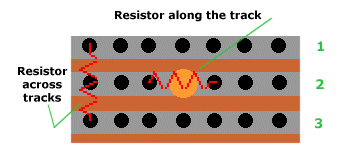
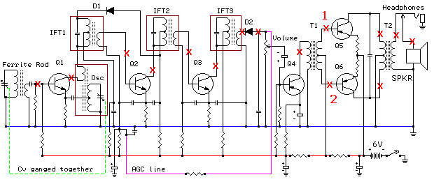
Let's look at a typical transistor AM Radio Receiver schematic shown in Fig 7 below. This you will note is one of my better creative efforts you must admit Commonsense dictates you would check the battery supply points at 10 and 11 (including to see if the on / off switch functions) to make sure the appropriate voltage is reaching the PCB. A typical radio is powered by four batteries of 1.5 volts (1V5 in my language) each so the total supply is 4 X 1.5 = 6V. If your radio has this then you check between points 10 and 11 with you multimeter on the DC scale to ensure you have 6V. If you get nearer to 4V then buy new batteries. If you still get much less than 6V then there is a dead short somewhere.
Assuming we get about 6V and our on / off switch functions O.K. then we move into our radio detective mode (gee! this is sooooo thrilling - me I LOVE it).
Put your probe at the most right hand point marked with the red "X" and press your button. Hear a tone? GOOD. Now proceeding from right to left at points red "X" - still hear a tone through the speaker. Yes GOOD or, if NO then put your probe in turn on both speaker terminals. NO tone = dud speaker or something dodgy with the headphone socket. Tone through speaker itself but NO tone through the base of either transistor (points 1 and 2) indicates a problem around the particular transistors or perhaps even the transformer T2 itself.
Assuming all is O.K. so far, we simply move backwards (from right to left) through all the red "X" test points. It's as simple as that. Pure detective work, looking for clues.
All you are doing is localising the problem area. Having localised the area, then troubleshooting it is the subject of another tutorial entirely. This one was long enough.
I've given you some hints, tips and yet in other areas I've left a lot to your imagination but that's what it's all about, that's the way it should be - this is YOUR creation, not mine!!!!
If it works - TAKE PRIDE IN YOUR ACHIEVMENT - if it doesn't work, don't despair because it happens to all of us. Simply don't give up, put it aside and come back tomorrow with a fresh mind and review all that you have done or forgot to do.
In writing this particular tutorial and preparing the associated graphics it took me about 40+ hours spread out over 4 days (including 12 hours straight the first day). The first point of that statement is this - I uncovered 27 different mistakes and omissions I had made over that time. The second point I want to make, particularly to youngsters, is my motto "winners NEVER quit and quitters NEVER win". Think about it.
Please do let me know how you get on, I'm always very interested. Get yourself on my monthly email newsletter for updates and how about telling a friend or your school about my site? I'm always willing to help schools and colleges out.
Consider printing out an extra copy of this project for your science teacher!
FREE Monthly Newsletter - keep up to date with site improvements and additions here. You can View
the previous issues. Concerned over privacy issues? If so please read my firm policy commitment on "your privacy and quickly unsubscribing" from my FREE Monthly Newsletter. If you have got this far then send me an email - put yourself on my update newsletter if you want, doesn't cost anything and I'll let you know what's happening.
FINALLY FOR CONSTRUCTING
BUT DOES IT WORK?
HOW TO USE YOUR MULTIVIBRATOR SIGNAL GENERATOR
![]()
Revised 6th January, 2001
My privacy statement
Subscribe to my FREE monthly Newsletter
Email to: Ian C. Purdie
URL: http://my.integritynet.com.au/purdic/square-wave-generator.htm
Copyright © 1998-1999-2000-2001 by Ian C. Purdie