

Hutton Close, Crowther Ind Est, Washington, Tyne & Wear NE38 0AH, England
Email: enquiry@isocomoptocouplers.com - Tel: +44 (0)191 4166546 - Fax: +44 (0)191 4155055
Hutton Close, Crowther Ind Est, Washington, Tyne & Wear NE38 0AH, England
Email: enquiry@isocomoptocouplers.com
- Tel: +44 (0)191 4166546 - Fax: +44 (0)191 4155055
Circuit and Package
Features
Description
Absolute Maximum
Ratings
Electrical Characteristics
Switching Characteristics
Similar Optocouplers
Home
Page
| Units: mm | DIL | ||
|---|---|---|---|
 |
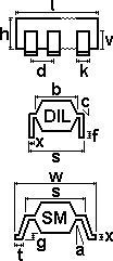 |
a | 0-13 degrees |
| b | 6.10-6.60 | ||
| d | 2.54 Typ | ||
| f | 3.29 Min | ||
| h | 3.25-3.75 | ||
| k | 0.48-0.56 tip,1.1-1.4 shoulder | ||
| l | 9.40-9.90 | ||
| s | 7.62 Typ | ||
| x | 0.20-0.30 |
High Current Transfer Ratio 800% Typical
Low Input Current Requirement
0.5 mA
TTL Compatible Output 0.1V Vol
Withstand Test Voltage 3000Vdc
High
Common Mode Rejection 500V/µs
Guaranteed Performance Over Temperature 0°C
to 70°C
Base Access allows Gain Bandwidth Adjustment
High Output
Current 60mA
DC to 1 Mbit/s operation
The 6N138 and 6N139 high gain series couplers use a Light Emitting Diode and
an integrated high gain photon detector to provide 3000Vdc electrical
insulation, 500V/µs common mode transient immunity and extremely high
current transfer ratio between input and output. Separate pins for the
photodiode and output stage result in TTL compatible saturation voltages and
high speed operation. Where desired, the Vcc and Vo terminals may be tied
together to achieve conventional photodarlington operation. A base access
terminal allows a gain bandwidth adjustment to be made. Surface Mount Option Available.
All electrical
parameters are 100% tested. Specifications are guaranteed to a cumulative 0.65%
AQL.
Absolute Maximum Ratings (25°C) | |
| Storage Temperature: | -55°C to +125°C |
| Operating Temperature: | 0°C to +70°C |
| Lead Soldering: | 260°C for 10s, 1.6mm below seating plane |
Input Diode | |
| Average Current IF: | 20mA |
| Derate Linearly: | 0.4mA/°C above 50°C free-air temperature |
| Peak Current IF: | 40mA (50% duty cycle, 1ms p.w.) |
| Peak Transient Current IF: | 1.0A (p.w.<=1µs, 300pps) |
| Reverse Voltage VR: | 5V |
| Power Dissipation: | 35mW |
| Derate Linearly: | 0.7mW/°C above 50°C free-air temperature |
Output | |
| Current IO(pin 6): | 60mA |
| Emitter-Base Reverse Voltage (Pins 5-7): | 0.5V |
| Supply and Output Voltage VCC(pin 8-5), VO(pin 6-5): | 6N138: -0.5V to 7V 6N139: -0.5V to 18V |
| Power Dissipation: | 35mW |
| Derate Linearly: | 0.7mW/°C above 50°C free-air temperature |
Caution: The small junction sizes inherent to the design of this bipolar component increases the component's susceptibility to damage from electrostatic discharge. Normal static precautions should be taken in handling and assembly of this component to prevent damage or degredation.
Electrical Characteristics(Over recommended temperature Ta= 0°C to 70°C u.o.s.; all typical values at Vcc=5V, Ta=25°C u.o.s.) | ||||||||
| SYMBOL | PARAMETER | CONDITIONS | PART | MIN | TYP | MAX | UNIT | NOTES |
|---|---|---|---|---|---|---|---|---|
| CTR | Current Transfer Ratio | VO=0.4V, VCC=4.5V, IF=0.5mA | 6N139 | 400 | 800 | % | 1,2 | |
| VO=0.4V, VCC=4.5V, IF=1.6mA | 6N139 | 500 | 900 | % | ||||
| 6N138 | 300 | 600 | % | |||||
| VOL | Logic Low Output Voltage | VCC=4.5V, IF=1.6mA, IO=6.4mA | 6N139 | 0.1 | 0.4 | V | 2 | |
| VCC=4.5V, IF=5mA, IO=15mA | 0.1 | V | ||||||
| VCC=4.5V, IF=12mA, IO=24mA | 0.2 | V | ||||||
| VCC=4.5V, IF=1.6mA, IO=4.8mA | 6N138 | 0.1 | V | |||||
| IOH | Logic High Output Current | IF=0, VO=VCC=18V | 6N139 | 0.05 | 100 | µA | ||
| IF=0, VO=VCC=7V | 6N138 | 0.1 | 250 | µA | ||||
| ICCL | Low Level Supply Current | VCC=5V, VO=open, IF=1.6mA | 0.2 | mA | ||||
| ICCH | High Level Supply Current | VCC=5V, VO=open, IF=0mA | 10 | nA | ||||
| VF | Input Forward Voltage | TA=25°C, IF=1.6mA | 1.4 | 1.7 | V | |||
| BVR | Input Reverse Breakdown Voltage | TA=25°C, IF=10µA | 5 | V | ||||
| dVF/dTA | Input Diode Temperature Coefficient | IF=1.6mA | -1.8 | mV/°C | ||||
| CIN | Input Capacitance | VF=0, f=1MHz | 60 | pF | ||||
| IIO | Input-Output Insulation Leakage Current | RH=45%, TA=25°C, t=5s, VIO=3000Vdc | 1.0 | µA | 3 | |||
| RIO | Resistance | VIO=500V | 100 | Gohm | ||||
| CIO | Capacitance | f=1MHz | 0.6 | pF | ||||
Switching Characteristics (Ta=25°C, Vcc=5V) | ||||||||
| SYMBOL | PARAMETER | CONDITIONS | PART | MIN | TYP | MAX | UNIT | NOTES |
| tPHL | Propagation Delay Time to Logic Low at Output | IF=0.5mA, RL=4.7kohm | 6N139 | 5 | 25 | µs | 2,4 | |
| IF=12mA, RL=270ohm | 0.2 | 1 | µs | |||||
| IF=1.6mA, RL=2.2kohm | 6N138 | 1 | 10 | µs | ||||
| tPLH | Propagation Delay Time to Logic High at Output | IF=0.5mA, RL=4.7kohm | 6N139 | 5 | 60 | µs | ||
| IF=12mA, RL=270ohm | 1 | 7 | µs | |||||
| IF=1.6mA, RL=2.2kohm | 6N138 | 4 | 35 | µs | ||||
| CMH | Common Mode Transient Immunity at Logic High Level Output | |VCM|=10Vp-p, RL=2.2kohm, RCC=0, IF=0mA | 500 | V/µs | 5,6 | |||
| CML | Common Mode Transient Immunity at Logic Low Level Output | |VCM|=10Vp-p, RL=2.2kohm, RCC=0, IF=1.6mA | -500 | V/µs | ||||
1. DC Current Transfer Ratio is the ratio of output collector current Io to
the forward LED current If, times 100%.
2. Pin 7 Open
3. Device
considered as two-terminaled: pins 1,2,3,4 shorted together and pins 5,6,7,8
shorted together.
4. Use of a resistor between pin 5 and 7 will decrease
gain and delay time.
5. CMh is the maximum tolerable common mode transient
to assure that the output will remain in a high logic state (ie. Vo > 2.0V).
CMl is the maximum tolerable common mode transient to assure that the output
will remain in a low logic state (ie. Vo < 0.8V).
6. In applications
where dV/dt may exceed 50000V/µs (such as static discharge) a series
resistor Rcc should be included to protect the detector IC from destructively
high surge currents. Recommended value:
RCC (kohm)=(1V)/(0.15 IF (mA))
Isocom takes great effort to ensure accurate data, but regrettably cannot be held liable for any error on its website. Visit File Lists to confirm old printouts are up-to-date.