Similar structures have been proposed on diamond, too, another possible candidate for detectors in the future (see [Bauer96]).
After the first implementation of a planar technology in 1980 [Kemmer80], semiconductors were quickly understood to give detectors of extraordinarily high performance. Recent progress in microtechnology now allows reliable large-scale production of detectors of sophisticated designs, at acceptable cost; their properties have been pushed to:
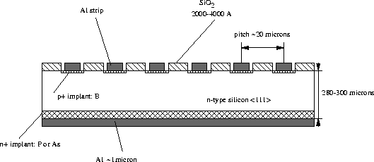
The principle of operation of a semiconductor detector is the following: if an ionizing particle penetrates the detector it produces electron-hole pairs along its track, the number being proportional to the energy loss. An externally applied electric field separates the pairs before they recombine; electrons drift towards the anode, holes to the cathode; the charge is collected by the electrodes (charge collection). The collected charge produces a current pulse on the electrode, whose integral equals the total charge generated by the incident particle, i.e. is a measure of the deposited energy. The readout goes through a charge-sensitive preamplifier, followed by a shaping amplifier. Silicon detectors are asymmetric p-n junctions; to work as a detector, the p+n diode is reverse-biased by applying a positive voltage on the rear ohmic contact, a metal deposited on the n side. At full depletion, the electric field is a maximum in the junction and decreases to zero at the ohmic contact. In order to avoid losses in charge collection, the silicon detectors are overbiased (below break-down voltage).
The intrinsic energy resolution is related to the low energy threshold:
only 3.6 eV are necessary to produce an electron-hole pair, a low value compared to the ionization energy in a gas (30 eV) or the approximately 300 eV necessary to extract an electron from a photocathode coupled to a plastic scintillator.
The good spatial resolution comes from the high density of Si, which reduces the range of the secondary electrons. On the other hand, the average energy loss in Si is high, about 390 eV/ ![]() [Barnett96],
for a <1 1 1>
oriented single crystal, and corresponds to about 110 e-h pairs. To limit the multiple Coulomb scattering, the detector thickness must be kept thin;
the usual compromise thickness is
[Barnett96],
for a <1 1 1>
oriented single crystal, and corresponds to about 110 e-h pairs. To limit the multiple Coulomb scattering, the detector thickness must be kept thin;
the usual compromise thickness is ![]() for optimum detection.
The thickness of the detector also determines the amplitude of the signal, as there is no charge multiplication in silicon; the signal-to-noise ratio is, therefore, a critical issue. For 300
for optimum detection.
The thickness of the detector also determines the amplitude of the signal, as there is no charge multiplication in silicon; the signal-to-noise ratio is, therefore, a critical issue. For 300 ![]() , one gets on average
, one gets on average ![]() electron-hole pairs, a signal requiring low-noise electronics.
electron-hole pairs, a signal requiring low-noise electronics.
The high particle fluence in the interaction regions of colliders is a critical parameter for the operational parameters and detector performance ( ![]() Radiation Damage in Semiconductors).
Radiation Damage in Semiconductors).
The crystals (wafers) from which the detectors are composed,
are produced by specialized companies.
Silicon is a IV group element in the periodic table. In the intrinsic material the electron and hole densities are equal; at room temperature ![]() cm-3.
Materials of p or n type are obtained by replacing some silicon atoms with atoms of the III group, or V group, respectively.
cm-3.
Materials of p or n type are obtained by replacing some silicon atoms with atoms of the III group, or V group, respectively.
Doping, via the charge carrier concentration, determines the resistivity ![]() of the semiconductor material.
Detector-grade silicon has very low doping, i.e. high resistivity (
of the semiconductor material.
Detector-grade silicon has very low doping, i.e. high resistivity ( ![]() ,
, ![]() cm). Float-zone n-type material is produced from silicon with minimum boron concentration,
by repeated zone refining to reduce the phosphorus concentration [Dreier90].
cm). Float-zone n-type material is produced from silicon with minimum boron concentration,
by repeated zone refining to reduce the phosphorus concentration [Dreier90].
Nuclear physicists widely use P-I-N structures along with p+n diodes. Doped detectors like Ge(Li), Si(Li) are also common. Surface barrier detectors (e.g. Au deposited on silicon) have been used in calorimetry, e.g. at H1 at HERA, see [Fretwurst96].
Basic references to semiconductor devices are [Lutz95] and [Sze81].