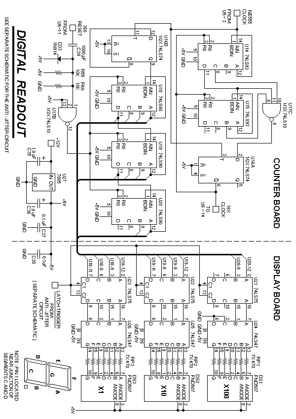
BEARING COUNTER
These three decade counters will not ( automatically ) "rollover" to zero, whenever their total number reaches 360... they must be externally "reset" to zero when this number is reached. That is achieved by tapping into the "D" bit of the original ( divide by 16 ) counter, located on the main board. The falling edge of this particular signal occurs ONLY when the divide - by - 16 counter "rolls over" to zero. Obviously, both counters should always read "zero" simeltaneously, so "tapping in" to this signal will do the trick. The RC network and inverter is required to produce a very brief pulse ( of proper polarity ) to drive the "reset" inputs of the bearing counter.
CLOCK CIRCUIT
For example, if a common clock of 360 KHz is used, dividing it by 45 will yield a clock of 8 KHz. This can be applied to pin 14 of the 74LS93 on the original ( main ) board, which will further divide it by 16, to yield an antenna rotation rate of 500 revolutions per second. ( = 500 Hz ) Dividing the same 360 KHz clock by 2 yields a frequency of 180 KHz, which can be applied to the input of the divide - by 360 counter of the digital display. Dividing 180 KHz by 360 also yields 500 Hz... identical to the rotation rate of the antenna.
In other words, 45 x 16 = 2 x 360
The divided - by 2 circuit ( U16B ) is simple, and requires no explanation. The divided - by - 45 circuit consists of a pair of 4 - bit counter chips ( U14 and U15 ) and a NAND gate ( U17A ) that detects when these counters have reached a count value of 44. A single D - type flip - flop ( U16A, driven by the NAND gate ) is normally triggered into the logic "1" state, ( Q = high, /Q = low ) and is triggered into the logic "0" state ONLY by the 45th clock pulse. Once the D flip - flop is triggered to logic "0", it’s inverted output ( on pin 6 ) goes high and resets both of the 4 - bit counters to zero. This will cause all the NAND gate inputs to go low, so the output of the NAND gate will go high.
The next clock pulse ( number 46, or number "zero" of the next cycle ) will trigger the D flip - flop back to logic "1" ( because the D input is again "high" ) and this will re-enable the 4 - bit counters. NOTE : The 4 - bit counters trigger on the falling edge of the clock, but the D - type flip - flop triggers on the rising edge of the clock. This prevents any "race" conditions.
"ANTI - JITTER" CIRCUIT
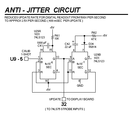
The circuit consists of a pair of monostable flip-flops, ( 1-shots ) with different pulse durations. IC U29A has a duration of ( approx. ) 4 microseconds, and is triggered by the CALIB 1-shot, located on the MAIN board. The output of this 1-shot is used to trigger the 74LS75 data latches on the NUMERIC board. It also triggers the second 1-shot, ( U29B ) which has a duration of ( approx. ) 0.4 seconds. While U29B is triggered, it inhibits further triggering of U29A by holding its /RESET input low. ( pin 3 )
If you want to change the update rate, do not decrease the value of R62 below 2.2K or damage to the IC might result. Values above 50K are discouraged by the chip manufacturer, because the resulting pulse length will become excessively sensitive to temperature, and ( in an extreme case ) the pulse lengh may become "infinite"... the 1-shot will fail to reset to its "untriggered" state.