New ways to Increase Sensitivity to Weak Signals, and
some Quantitative Insights into Diode Detector Operation,
derived from Simulation in SPICE.
By Ben H. Tongue
Quick Summary: Very low signal
sensitivity of a crystal set can be improved by cooling the diode. This
effect starts being effective when the rectified current is below about
twice the Saturation Current of the diode.
Part 1.
This Article will show some quantitative information about diode detector
operation that has been abstracted from SPICE simulation and curve fitting.
One can determine, for a diode detector:
-
When the detector is operating at the Linear-to-Square-Law Crossover Point
(about 5 dB insertion power loss).
-
Detector insertion power loss as a function of input power or rectified
current.
-
Output power as a function of input power.
-
How to increase weak signal sensitivity.
Definitions of terms to be used
Plsc(i) Input power at the linear-to-square-law
crossover point
Plsc(o) Output power at the linear-to-square-law crossover
point
Is Saturation
current of the diode
n
Ideality factor of the detector
DIPL Detector insertion power loss
Pi Available
input power
Po Output power
sqrt Take the square root of the
following expression
Kt Temperature in degrees
Kelvin
C Temperature in degrees
Celsius
Ri Detector input
resistance
Ro Detector output
resistance
R1 Source resistance
R2 Load resistance
I2 Rectified
current
The diode detector circuit we will refer to is shown in Fig. 1.
Fig. 1
Assumptions:
-
The Q and L/C ratio of tuned circuit T are assumed to be high and
low enough, respectively, so that the 'flywheel effect' of T prevents
any appreciable clipping of the positive voltage wave form peak by diode
D1.
-
The value of C2 is assumed to be high enough so that only a negligible
amount of RF voltage appears across it.
-
The diode parameters Is and n are known from measurement or a Data Sheet.
A simplified method of estimating Is is given in Section 2, Article #4,
but the parameter n has to be estimated. A method for measuring both
Is and n is given in Article #16. The effect of the series bulk resistance
of the diode is assumed to be negligible - as it is at low signal levels
for most all diodes. Diode back leakage current from either 'parasitic
leakage' or operation with voltage swings reaching into the 'reverse breakdown
current' region is negligible. The diode temperature will be assumed
to be 25 degrees C. in Part 1.
Approach: The RF signal power range will be divided into three areas
or regions, and impedance and power relationships will be determined.
Refer to Figs. 2 and 3.
-
The low power region: Here, the relation between output power and
input power is 'square-law'. That is, for every one dB change in
input power there is a two dB change in output power.
-
The high power region: Here, the relation between output power and input
power is 'linear'. That is, for every one dB change in input power
there is a one dB change in output power.
-
The area between the linear and square law regions, centered on the 'linear-to-square-law
crossover' point. That is, for every one dB change in input power
there is a 1 1/2 dB change in output power.
Transition from the linear to the square law region: All diode
detectors, at high input power levels, if well impedance matched at input
and output, have a low insertion power loss (a fraction of a dB).
If the input power level is then reduced, at first the output will drop
dB for dB in step with the input. As the input is further dropped,
the output will start to drop faster (in dB). This can be thought
of as the onset of 'detector insertion power loss'. When the input
power equals the that at the LSC point, about 5 dB insertion power loss
occurs. In a crystal set, if the output audio power is now so low
that one can't hear anything in the headphones, one probably doesn't care
(except if recovery of that 5 dB loss were possible). Reception of
lower power signals where insertion power loss increases at a rate approaching
2 dB for every one dB of input signal reduction seems hopeless.
If one can read signals of around Plsc(i) Watts, it would obviously
be desirable to lower the input power at which the LSC point occurs so
that more of the weak signals would be closer to the linear mode of operation
and therefor experience less insertion power loss.
Detector input and output resistance considerations: The input
and output resistances of the diode detector are: Rin = Rout = 0.0256789*n/Is
ohms, approximately 700k ohms in the following example. Assume that
the source and load resistances are 700k ohms. Figs. 2 and 3 show
power relations at various power levels with the LSC point shown by
an arrow.
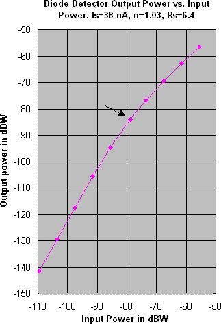 |
 |
Fig. 2 - A SPICE simulation of the relation
between output and input power.
|
Fig. 3 - Data from a SPICE simulation showing
detector insertion power loss vs. input power.
|
Assume that the source and load resistances are each: 0.0256789*n/Is
ohms. This establishes a very good input and output impedance match
at low signal levels and a moderate match at high levels.
SPICE simulation and curve fitting shows that operation at the LSC point
occurs when the diode rectified current equals: I2=2*Is.
(1)
A curve that fits the relation between output and input power quite
well over the whole range of the graph in Fig. 2 is: Po=20*log[sqrt(0.10272*n*Is+Pi)-sqrt(0.10272*n*Is)]
dBW. (2)
A curve that fits the detector insertion power loss (DIPL) quite well
over the whole range of the graph in Fig. 3 is:
DIPL=20*{log(sqrtPi)-log[sqrt(0.10272*n*Is+Pi)-sqrt(0.10272*n*Is)]}
dB. (3)
An equation that uses rectified current instead of input power and gives
the same result is: DIPL=10*log(I2/(I2+4*Is)) dBW.
(4)
The input power at the LSC point is: Plsc(i)=10*log(0.3081*n*Is)
dBW. (5)
The output power at the LSC point is: Plsc(o)=10*log(0.1027*n*Is)
dBW. (6)
The ideality coefficient of the diode is an important parameter in determining
very weak signal sensitivity. If all other diode parameters are kept
the same, the weak signal input and output resistances of a diode detector
are directly proportional to the value of n. Assume a diode with
a value of n equal to oldn is replaced with an identical diode, except
that it has an n of newn, and the input and output impedances are re-matched.
The result will be a detector insertion loss change of: 10*log(oldn/newn)
dB. That is, a doubling of n will result in a 3 dB drop in power
output, assuming the input power is kept the same. This illustration
shows the importance of a low value for n.
Part 2.
How might all this be used to increase the weak signal sensitivity
of a crystal set?
Assume that a station one can barely read has a power sufficient only
to operate the detector at or below the LSC point (the point where the
rectified diode DC current is two times Is). The volume will be increased
if the lsc(i) point can be made to occur at a lower RF power level.
This will result in less insertion power loss since operation will now
be closer to the linear region. The required power at the lsc(i)
point can be rewritten as: Plsc(i) = 10*log (0.0001034*Is*n*Kt)
dBW. Kt = Temperature in degrees Kelvin. One can see
from the equation that if Is, n or Kt can be lowered, the lsc(i)
point is lowered and the volume from weak signals can be increased.
It has been shown that in any particular diode, any % drop in Tk will automatically
result in a much larger % drop in its Is. It must be remembered that
the reduction of Is or Kt increases Ri and Ro. If n is reduced,
Ri and Ro are reduced.
-
Reduction of Is: The main limit to reduction of diode Is has
to do with the resultant increase in RF input (Ri) and audio output (Ro)
resistances of the detector and their practical low loss realization.
At input signal levels at or below the lsc(i) point, those values are about:
Ri
= Ro = 0.0000862*n*Kt/Is ohms. The example in Figs. 2 and
3 are for a case where Ri and Ro both equal 700k ohms, using a diode with
an Is of 38 nA and an n of 1.03. This is close to the limit of practicality
and applicable mainly in crystal sets using a single tuned, high inductance,
high Q loop antenna with a high quality, high transformation ratio audio
transformer. A practical value for R2 for most crystal sets is about
330k ohms (requiring a diode with an Is of about 80 nA for a good impedance
match). This raises the Plsc(i) by about 3 dB and reduces
the output of signals that are well into the square law region by about
3 dB. Signals well above the LSC point are hardly affected at all.
-
Reduction of n: The value of n can vary quite a bit even among
diodes of the same type. Schottky diodes usually have a low value
for n. Probably so called 'super diodes' have a low n and their values
of Is and n are such that a good impedance match is realized in the particular
crystal set used.
-
Reduction of Kt: The temperature of the diode can be lowered
by spraying it with a component cooler spray (221 degrees K.) every so
often. A longer lasting, but lesser cooling can be had if the diode
is placed crosswise through two diametrically opposite small holes in a
small housing (such as a 1'' dia. by 2.5 inch long plastic pill container)
with a stack of copper pennies in the bottom to act as a thermal mass.
This assembly is used by first placing it in a home freezer for cooling
to about 0 degrees F. (255 degrees K.). It is then taken out and
connected in the crystal set. An even lower temperature can be attained
if some pieces of dry ice (195 degrees K.) are substituted for the pennies.
The problem with reducing Kt is that Is is very temperature sensitive.
Agilent states in App. note #1090 that the junction resistance of HSMS-2850
Schottky diode increases 100 times for a 70 degree K. reduction in temperature.
That indicates a much greater % drop in Is than in Kt if Kt is reduced.
A 70 degree K. temperature drop may reduce the Is by 100 times, raising
Ri and Ro by 100 times. That ruins impedance matching and increases
loss greatly (the signal goes away). The answer is to experimentally
try diodes that have a high Is at room temperature (298 degrees K.), that
will drop to the correct value at the reduced temperature. One candidate
is the Agilent HSMS-2850 (room temperature Is = 3000 nA). Another
is a 2N404A Ge transistor with the base and collector leads tied together
(room temperature Is = 1500 nA).
These suggestions probably won't help unless high sensitivity phones are
used because the audio signal will be weak. A low loss audio transformer
will be needed to transform the impedance of the phones up to the value
of R2. Also, the DC load on the diode should be the same as the AC
load. This can be accomplished by placing a bypassed resistor of
value equal to R2 in series with the primary of the transformer.
See other information on diode detectors and transformers in Articles #0,
1, 4, 5, 10, 15 and 16.
This information points a way to increase the sensitivity of some crystal
sets to weak signals. If the crystal set and headphone combination
is lossy enough so that a signal of strength at least equal to Plsc(i)
cannot be heard (rectified current = 2*Is), this information probably won't
help.
Published: 04/10/01; Revised: 05/20/01
Return to Home Page
|
