Manhattan Style Construction Ab Initio

by Chuck Adams, K7QO

k7qo@primenet.com

http://www.qsl.net/k7qo

Last Updated January 1st of 2000.

This is now the completed article. Critiques are welcome and changes to be made need to be made ASAP. Thanks.


This article is intended to give you an overview of construction techniques for homebrewing and then give significant detail on what is called the Manhattan Style of construction. At the beginning of each section is a brief paragraph outlining the discussion topic for that section. Also note that I will summarize materials and tools requirements at the end so you don't have to take too many notes as you go along. You might want to take notes as you read anyway. It will help you concentrate on the material and remember it significantly longer.

I recommend that you read through this complete article several times before embarking on building and experimenting just to make sure that you have everything on hand before you get started. If you are like me, you hate to start on something, be interrupted and then have to to go and get something that you are missing or have overlooked. Plan ahead and you will save a lot of valuable time. All the suggestions within this article are just that --- suggestions. So feel free to add or take away where you have something that you have learned or want to use in place of my ideas or tools.

Introduction to Construction Techniques

This section gives a description and pointers on different construction techniques. In the reference materials you'll find some excellent ideas with figures and photographs to further your education and add to my discussion.

Lately in the QRP world there is an increased interest in basic construction techniques and the "Manhattan Style" of construction in particular. It is my hope that this article will bring to light some basic understanding of just what is involved in building with this technique. To make this article of interest for all ages and building experiences, I ask for your patience while I start from the basics and work up to the more complex issues.

If you have a copy of the ARRL Handbook [http://www.arrl.org/] for 1995 or later, please get it out and read the first part of the chapter on construction techniques. This is chapter 25 and you only need to look at the first 12 pages for our discussion here. You will note that Figures 25.10 through 25.22 illustrate the most popular techniques for building circuits. You can use these techniques for experimentation or for final components of a rig or for a complete receiver, transmitter, or transceiver. These techniques consist of:

  • Ugly Construction,
  • Wired-Traces Construction,
  • Terminal-and-Wire Construction,
  • Perforated Board Construction or Perf Board for short,
  • Solderless Prototyping Board,
  • Perf Board and Wire-Wrap Construction,
  • Etched Printed Circuit Board, and
  • Glued Copper Traces on Printed Circuit Board, which we will call Manhattan Style Construction.

    Each of these techniques is excellent for the construction of test circuits, etc. Don't let anyone whine and tell you that one is any better than the others or that they have never gotten one of the techniques to work and you won't either. Have you ever noticed that people that you never hear from for long periods of time all of a sudden come out of the woodwork and claim to be an expert and are ready to give you advice which you neither asked for nor need? Just an observation over the years. Yes, in some cases like VHF and UHF some construction techniques will give you problems if you lack experience, but we are talking only HF here in this article. I have used all of the above techniques and each works. Some just take more care in dealing with component placement and routing of critical signals and voltages. One designer that I know of has built a complete 2 meter SSB transceiver on a Radio Shack solderless prototyping board, so VHF gear can be built using these techniques.

    I will cover the basics of the Manhattan Style of construction here. If there is continued interest, then send email to George Heron, Editor in Charge, to show support for more articles of this nature in QRP Homebrewer. Look for his current email and address information on the inside cover of this issue. I would like to follow up this article with another using the Dave Benson's NN1G Mark II transceiver as a discussion for building a more complex design using Manhattan style construction and also as a tutorial for just how a transceiver works. Something that I wanted to do in a advanced Elmer series.

    In the ARRL publication "QRP Classics" there are two articles that you should read at this time if you have a copy. This book is out of print and you should look for a copy at swapmeets and hope that you run across it. It is a collectors item. If you do not have a copy, then reference the original article in QST either in hardcopy or on the ARRL CDs. The first is from the September 1979 issue of QST, page 30, written by Doug DeMaw, W1FB. The title of the article is "Quick-and-Easy Circuit Boards for the Beginner" detailing construction using what is referred to as dead bug or ugly construction. To support various component leads and connections that are not directly connected to ground he uses high resistor values on the order of several million ohms. The support resistors are soldered in a vertical position with one end to the printed circuit board and the upper lead is used to hold several connecting leads. This resistor provides good isolation from the ground point through a relatively high resistance. This upper resistor lead also provides a mechanical and electrical connection that gives excellent mechanical stability for the final circuit configuration. The problems with this technique are that I find is that you must have a supply of high valued resistors (on the order of 1 megohm or more) and thus an additional cost to the completed circuit or project and I personally find that the extra work to bind the leads together and solder them is sometimes time consuming and just plain tedious work to get a good and nice looking connection. And for my projects I figure that if I am going to spend the time and money in constructing something then I might as well do a good job and wind up with something that looks as nice as it works. It is much much faster and easier for me to make a nicer looking project using the Manhattan Style of construction.

    In the same article by Doug DeMaw, Figure 3 shows the use of printed circuit board squares glued to the main printed circuit board. The squares are used to solder component leads to for common electrical and mechanical connections. This technique is attributed to Wes Hayward, W7ZOI, and Wes suggested using hot glue as a fixitive to hold the pads in place. Comments are made about the extra care needed as the hot glue softens each time a component is soldered to the pad(s). I have yet to find a technique that repeatedly results in equal amounts of hot glue for each pad. I am not a fan of this technique for that reason and my favorite glue is Super Glue (cyanoacrylate glue) found at hobby shops and at many other stores for holding pads down. And because of my fondness for uniformity and order I prefer circular pads over rectangular or square pads. I haven't developed a technique or found a tool for making such pads that are consistent in shape and size.

    The other article in "QRP Classics" is one also by Doug DeMaw from the September 1981 issue of QST page 11. The article "Experimenting for the Beginner" has some excellent circuits including the W7ZOI QRP transmitter that can easily be built using the Manhattan Style construction technique described in this article. In fact, if you have been collecting schematic diagrams and articles over the years or decades (and I know you have), then now is the time to start in building them and experimenting as you have hoped to do all this time. There are two main reasons why I suggest you do this now. You'll collect, if you haven't already, more projects than you will ever have time to build in one lifetime. Also, the parts are much easier to find for the projects now as we are closer to the publication date. At a much later time the supply of some parts will dry up due to the nature of the electronics business and where it is going. And it naturally follows that the pricing will go up as the vendor must reserve valuable space for storing items and they must pass the added expense for this on to you. This increased cost of some items will also increase your cost of doing a project.

    Now for some of the history as I know it for the term "Manhattan Style Construction".

    At Dayton several years ago there was a building contest sponsored by the NorCal QRP Club that consisted of building a complete transceiver using only 2N2222 transistors. The idea came from Wayne Burdick, N6KR. I was one of the judges for that contest at Dayton that year. The first place winner was Jim Kortge, K8IQY, with a 40 meter transceiver completely made up of only 2N2222 transistors with no IC chips to be found anywhere in the design. He built the rig using the Manhattan Style technique and he used the phrase which his son used in college in an engineering program where they built this way. Since the contest at least 16 of the K8IQY rigs have been built using the same construction technique and used on the air to make contacts and the number is growing. You can see Jim's work at http://www.qsl.net/k8iqy if you have Internet capabilities. It is worth the time and effort to visit the site. Jim is currently working on a 15 meter version of the same rig with modifications and enhancements. Jim Kortge is showing all his work online during the development and construction phases thus giving you insight into how one person does rig design and testing.

    In case you are late in getting this article, all this work is taking place starting in late October of 1999.


    Printed Circuit Board Material

    In this section I will talk about printed circuit board material and tools for working with it to cut pieces to size for use in building circuits.

    One thing that you are going to need first off is a supply of printed circuit board material. In some cities this is readily available from electronic surplus stores such as Tanner Electronics in Dallas, TX. Since leaving Dallas I have grown to appreciate such places that I no longer have readily access to here in Prescott, but life is a series of tradeoffs. Radio Shack stores have printed circuit board material but you will find it more expensive than if you can find it at swap meets or ask around for sources locally. And then there is always the search over the Internet for parts places. I did find reference to double sided printed circuit board material at Dan's Small Parts web page --- http://www.fix.net/~jparker/dans.html and you need to directly check it to make sure the boards are still available and select the sizes that you want.

    It does not matter whether you use single sided or double sided material. Get that which is cheapest for you to obtain. I found some double sided board at Tanner Electronics in Dallas that is about 30cm by 60cm in size at a good price. It has a paper type dielectric and the copper coating is only 0.5 oz per square foot. But you don't care about the depth of the material for these projects. Printed circuit board material is rated by the density of the copper plating by 0.5, 1.0, and 2.0 oz per square foot. I use the 0.5 oz per square foot because it was relatively cheap and was the only thing that was in stock. The insulating substrate may be made of several different kinds of material. You do want something that you can use a nibbler or punch on rather easily. Some of the epoxy or fiberglass based material may require a significant force on the punch to make the holes and pads. I use the term pads to refer to the circular material that comes out of the hole made by the punch. Any other time you would just throw the hole material away. Don't do that here. We want to keep all the hole material. I'd recommend that you experiment here to find the material and board thickness that works best for you to make pads. It doesn't even have to be the same printed circuit board material you are using for the substrate or area on which to build. There are no hard and fast rules here.

    Once you get the board material the first thing that you want to do is to be able to cut it to the size required for each of your projects. This will require some planning on your part dependent upon what tools you have. Some builders use a hacksaw. Others use paper cutters (which will get dull rather rapidly on most printed circuit board material), metal cutting scissor-like tools, or a metal shear. Again I have done all three and my favorite is the metal shear. Harbor Freight Tools [http://www.harborfreight.com/] has a combination 12" shear, brake, and slip roll which sells for $199.95 and has a part number of 35969-1VGA. I managed to catch it on sale in Dallas for less than this, so check with them on current pricing. If you are fortunate enough to have a local store, be sure to take the opportunity to drop in sometime and take a look at the combination of shear and brake. I know that this is an expensive item, but it has more than paid for itself in enjoyment and in doing some nice work on printed circuit board material that I could not do otherwise. I have also used it for making the final cases on a number of projects using aluminum sheets. I'll write a section on just how to make the case(s) from aluminum sheets or printed circuit board material for your projects.

    I have also used a metal cutter made by Wiss with part number M-300 for cutting printed circuit board material. Be careful in buying this item as there are three cutters they manufacture and this particular one has orange handles and it will cut straight lines. The other two models are made to cut either right or left-handed curves and that is not what you want here. I bought my cutter at Home Depot, and it was priced at just under $15. I do not like using it for serious work as it leaves a small seratted edge on one side of the double-sided board, a minor nit if you want to save a lot of money on tools or start out slow before making the big leap and spend a lot of money on the higher quality tools used for homebrewing.

    IMPORTANT NOTE. No matter what technique you choose to cut the board material be sure the first thing that you do after cutting a board is to run a sanding block with medium to fine grained sandpaper along all the edges of the board to remove sharp metal edges and other sharp points from the dielectric material. The formed edges of the copper can make razor sharp edges and you want to take all the safety precautions that you can in working with this stuff. Please do not skip or forget about this step. It is very important. And please don't do something stupid like run your finger along the edge to see if it is sharp. You should be old enough to know better than to ever do this. I bring it up because you need to be thinking at all times when working with tools and materials. I use an extruded aluminum sanding block that I bought at a hobby shop. I use spray contact cement to apply sandpaper and by using the contact cement on one surface I can peel the used sandpaper away fairly easily.

    OK, you cut up the board to some rectangular size that you are going to build a circuit on. I recommend that you also make up several 5cm by 5cm boards for some experiments listed below just to get an idea of how to work with the construction techniques described here.


    Cleaning the Printed Circuit Board Surface

    In this section we come to the business of cleaning the copper plating on the printed circuit board.

    Depending upon your source of printed circuit board material you may find it either new or old. The copper plating will tarnish and oxidize over a period of time. This will require that you clean it. I even go through the process of cleaning for newly purchased board material. The best buy I have gotten on blank printed circuit boards was at Ft Tuthill a few years ago. The boards had some areas where it looked like they had been heated to a high temperature and were badly oxidized. This was most likely the reason why they were surplused out or rejected by someone. The cleaning technique discussed here does work and cleaned them up nicely.

    Here is what I have found to be the best cleaning technique for printed circuit board material. I ran a number of experiments with the cleaning products listed below. I went to several grocery stores and looked in the cleaning supplies section and visited hardware stores and even antique stores looking for copper and brass cleaners. My reasoning was that I needed some cleaning materials that were tested by a large population, certified over a period of time to be safe by both lawyers and the consumers, and would not harm me or the printed circuit board material for my projects. I'm sure if something would do damage it would have by now been pulled from the shelves. I wound up testing the following products:

  • Goddard's Brass and Copper Polish,
  • Brasso,
  • Gillespie Old Brass, and
  • Tarn-X.

    The product that worked the best and the one that also was the least expensive was Tarn-X. You should be able to find it in any large grocery store chain in the household cleaning materials section. Read the label carefully and completely and follow the instructions. I use a cotton ball and clean both sides of the board with the Tarn-X. I get the cotton ball wet with Tarn-X and wipe all the copper material until it is clean. Then I immediately rinse with plain tap water in the sink and then dry with a paper towel, all the while holding the board by the edges and not touching the copper surface. Do not allow the board to air dry with water spots as they will leave obvious markings on the surface of the board.

    You did sand the board edges, didn't you? You will always be handling the board by the edges. You will wind up with a shiny surface after cleaning the boards. I find that it doesn't seem to tarnish too rapidly, and I do nothing special after this treatment. Just avoid touching the surfaces of the copper plating with your fingers, etc. I have a technique also for avoiding contact with the board during construction and that is described in the building steps paragraphs. You might also consider using 1" masking tape folded over the edges of the board to protect you and the board while handling it. You can remove the masking tape after you have completed building.

    I prefer the Tarn-X as a cleaner as it is non-abrasive and works almost instantly upon contact. It doesn't require a lot of elbow grease, i.e. hard work or exercise, to get a clean surface without additional scratching. We are not trying for an optically flat surface but I don't like scratches produced by the abrasive compounds or steel wool. I would show a before and after photograph of the cleaning results, but the results do not photograph well. I'll let you experiment on your own and determine for yourself just how well the results look.


    Making Pads using Printed Circuit Board Material

    In this section I will describe how you can make the small pads that we will use for mounting components to the board and keep them isolated electrically from the ground plane.

    The next thing after making a board to be used for a project is to make up enough printed circuit board pads to use. Now Jim Kortge, K8IQY, has excellent results making very small rectangular pads. He uses an Adel Nibbler, which I don't think is being made any longer. I have searched far and wide and had no luck in finding one. I think in my younger days I had one but sometime over the years it disappeared. You know how that is with tools. I experimented using a Radio Shack nibbler and with the printed circuit board material that I had on hand. The pieces come out curved and won't lie flat on the printed circuit board. So I have what I think is the best tool for making pads. Jim Kortge, K8IQY, and others saw my work at Pacificon and thought that the pads looked good and worked well.

    Harbor Freight Tools has a 2,000 pound punch kit with part number 37405-1VGA. It sells for $15.99 and again I happened to catch it on sale when I bought mine. It consists of the punch with dies for making 2.38, 3.18, 3.97, 4.76, 5.56, 6.35, and 7.14 mm circular punches in metal or in this case printed circuit board material. I started with pad sizes of 4.76mm but now have settled on the smaller 3.18mm pad size. This size works best for me in saving room on the board, getting components closely spaced, and still large enough to easily solder several component leads to during construction. Remember that by pads I am referring to the material punched out of the printed circuit board, i.e. the circular sections that pop out of the punch. Also for using integrated circuits (and I always use sockets) with these sized pads, you can only do the corner leads (due to spacing) in what I call the "lunar lander" configuration. Probably for this reason alone a lot of people will tell you to go with the nibbler and the rectangular pads so that you can use pads for each of the leads. You can go with rectangular pads for the ICs or sockets and circular elsewhere but I just tack solder to the remaining leads of the socket with pads only on the four corners used to hold the IC socket to the printed circuit board, and this works well for me. In the detailed construction section I'll illustrate how I do this.

    Harbor Freight punch set front right.

    Now I made a modification to the punch that you may or may not want to try. I found that with the printed circuit board material I use, when I punched out the pads using the punch and dies, several things happened. There is a small raised point centered in each punch. This point holds and keeps the material being punched from moving laterally. The raised point made the pads concave and it also caused the copper to develop a fine hairline crack on one or both sides in the copper plating. I used an ordinary metal file and removed this center raised point. By removing the point the pads now come out rather nice and flat. Again, you may not want to do this as this is a permanent modification to the tool parts. Experiment with one of the punches. Try one punch size before and after this modification and see which configuration works best for you. If you don't like the results, then you have only made one modification to one of the punch sizes. You might want to use the smallest size to experiment with first as it will be the least likely candidate for making pads.

    Another thing that I bought at Harbor Freight is a 5" drill press vise. (Part number P31000 from Harbor Freight and again it is in the $15 price range, the same as the punch.) It is both heavy and sturdy and sits right on the desk top while in use and stores away in a relatively small space. I prefer it for most small work over a portable vise that clamps to a desk edge. I use this for holding all kinds of things while sanding, filing, etc. In using the punch to make printed circuit board pads I sometimes found it required considerable pressure. By putting the punch in the vise, I could exert more pressure and move along the printed circuit board material faster, thus punching out more pads in a shorter period of time. It is just something that I do, and you may want to wait on this purchase or use a vise that you already own.

    Harbor Freight vise.

    What I do is get some board material that is going to be large enough for me to make a hundred or so circular pads of the desired size. I make every attempt to cut the pads as close as possible to reduce the waste of board material. You have to practice to find the technique and procedure that works best for you. Be sure to clean this board material before you start in making the pads. This will make the pads nice and clean and shiny and easier to use.

    In the photograph showing this setup you will note that I use a small plastic container to collect the pads as they are punched so that I don't have to chase the little critters all over the desktop and floor. Been there. Done that. Also note that one or two pads may still be in the punch when you finish, so check before putting the tool back into its case for storage. I punch up a batch of pads at one time to maximize the number that I can punch for time and effort expended in setting up the tools. Experiment and let me know what works best for you. The plastic container is just a simple butter container that has been recycled for such use.

    Vice and punch setup for punching pads.


    Attaching Pads to the Printed Circuit Board

    In this section I will describe the technique and glue that I use for mounting the pads to the printed circuit board.

    Now after reading this article some people may consider me cheap. That is not the case, but sometimes I find that bargains are worth getting. Besides Harbor Freight I like to visit the everything-for-a-dollar thrift stores. They have some unusual stuff that might come in handy. I use their notebooks for keeping journals, logs, and QRP experimental notebooks. I also buy my super glue there for single tubes and sometimes two tubes for a dollar or less. Super glue does the best job for me of installing pads on the printed circuit board. Read the label on the glue and always be careful. Wear glasses or goggles at all times. A large number of us have seen discussions go on and on for threads on this topic on QRP-L. Super glue is just that, a glue, and every precaution should be used in applying it to the board, etc. I just love the stuff and if you experiment you can make a neat joint for the pad. I apply the glue to the printed circuit board at the point where I want the pad to go by placing a very small drop there. With care you can get the same size drop in the exact place you want it every time. Don't rush and don't use too much pressure. I hear the urban legends about mistakes and you don't want 35 hours into a big project lost due to a slipup on your part. Again, read the labels and be careful. I keep Acetone handy to clean up as needed.

    Some people will recommend that you go to a hobby shop and buy the large bottle of super glue that you can find there. I find that they are expensive and am concerned about the shelf life of the stuff. Keeping it in the refrigerator (which may be dangerous if you have children) is recommended by some people. Also note that you buy the glue in different set up speeds --- instant, regular and slow. These speeds give you different times in which to move the materials being glued together. You can experiment if you wish and decide which you prefer. As I say --- education is expensive no matter how you get it.

    I glue the pads as I make progress on the project. There is no need to get too far ahead as your placement and circuit details may change. I use the "build a section and then test it procedure" in a lot of my projects. By only placing pads as I go I do have the opportunity to modify the circuit and the layout on the board before it becomes too crowded and I don't have room to make the changes that I need. Some builders prefer to go ahead and lay out a project completely and do all the pads at one time to reduce time in setting pads and working with the glue. What you do is dependent upon your experiences and the techniques that you have developed or learned.

    You can "pop-a-pad" (tm de K7QO) with chain nose pliars with practice and clean the spot with Acetone. (Again for dangerous chemicals read the label and do it outside and upwind from the fumes. Acetone is highly toxic and volatile/flammable chemical found at any paint supplier.)

    I am hoping that you are reading this article through several times before you rush out the door and start buying stuff. While you are in Harbor Freight for the shear and punch ask them about item #32279. This is a $5.99 set of six tweezers that I just love to use not only for placement of pads but for picking up parts while building a kit and for retrieving parts dropped into a crowded board or case. You'll see what I mean after you get the set and use them for a while. You'll feel like a brain surgeon with a fine instrument. You can also find similar tweezers at some surplus vendors at hamfests like Dayton and HamCom. The tweezers are made of stainless steel, have very very fine points, and the super glue should not stick to them. Keep them out of the reach of children, please.

    I locate the spot on the printed circuit board where I want a pad to go. I then place a very small drop of super glue centered on the spot. I then use the tweezers to pick up a pad from my supply of pads and place the pad at the spot on the board. I GENTLY push on the top of the pad to seat it in the location I want and then hold the pad in place for about 5 seconds or so. The glue sets rapidly, but don't play here and test to see if the pad will move. If you haven't waited long enough, it will move and then you'll have a mess on your hands. Just be patient as the rewards are great. You'll get the hang of this after a few pad placements. I do put the pads with the smoothest side up.

    After another 15 seconds or so I then take the soldering iron and solder and tin the pad. I use just a little bit of solder. This process does two things. It pre-tins the pad for later soldering of component leads to it. It also helps "cure" the super glue under the pad and solidify the structure. Be careful not to use to much heat here and cause a portion of the super glue to vaporize. The fumes are not good for you. I use a small 12 cm by 12 cm computer fan (115VAC at 8W) near the work area to draw the fumes away from me and the work area. It is quiet and I have the soldering iron and the fan on a multi-outlet switched setup so that I can turn everything off with one switch. This keeps me from leaving the soldering iron plugged in and on for days at a time. Been there, done that. Don't have the fan blowing air across the work area unless you need the additional cooling during the summer months. Make sure that even in this configuration the fumes are not blown in your direction.


    Patented K7QO Soldering Technique

    In this section let's take a look at soldering and soldering tools and equipment as used at the workbench of K7QO in beautiful Prescott, AZ.

    Now the ARRL Handbook has some excellent information on soldering and the equipment needed, but I have my own way of doing things that have worked well for me over the years. Thank you for allowing me to share them with you.

    First of all, you do not need to spend an arm and a leg for a soldering iron. Yes, I know that the soldering stations sell for big bucks and are worth every penny spent on them. But, I have built over 125 kits in the last 7 years and built a lot of test circuits and odds and ends. All of this I have done with a simple Weller soldering iron model number SP-23. I would hazard an educated guess that they do not make it any more. It is a 25W iron with an Ungar tip (PL-823) that is also no longer being manufactured, but there is hope that you might find one in your searches through the piles of stuff at Dayton and other swap meets.

    Why do I like the tip? It has not degraded over the years with pitting, etc. It has a fine enough tip that I can do the smallest of soldering and it has flat surfaces large enough to provide both the surface area and thermal area to coat the thermaleze wire being used in most kits now for toroid windings.

    I bought a Radio Shack soldering iron stand at a hamfest somewhere and I think I paid $2 or so for it. It is the one with the small metal "sink" that holds a sponge. What most people do is have the sponge with a small amount of water to clean the tip of the soldering iron from time to time while working with it. You simply swipe the tip of the iron across the sponge and the process removes excess solder and flux on the tip of the iron. I dislike this physical process for two reasons. First of all it cools the tip slightly. Also the sponge tends to trap a glob of solder (like that high tech talk?) and then sling it in my direction while it is still molten and hot!! I consider this dangerous and an unpleasant experience when it happens.

    So what I do is the following. I always solder with blue jeans on. I recommend that you never solder while wearing short pants since you might drop the iron or something that is hot onto one of your legs. While soldering, I use a dry heavy or thick washcloth that I bought at a Wal-Mart or Target store. I place the wash cloth across the right pants leg as I am right handed. While soldering and when the tip has flux residue or too much solder on it, I just drag the soldering iron tip lightly across the wash cloth to clean it. I have been using the same cloth for over a decade with still no holes in it. Of course, you can't use it for anything else!! I'm sure some one will rant and rave about this, but I find it does a great job of cleaning the tip and it doesn't cool it down.

    Each of us has his or her supply of favorite solder. Over the past 6 years I was using a water soluable flux for all the kits that I built. I liked it because it was easy to cleanup with water and it was 63/37 solder that had a low melting point and it was eutectic. Eutectic means that it goes from a molten to solid state without going through a "plastic" stage. If the parts move during the time period when the solder is in a plastic stage you will get a connection that looks bad and will possibly be a cold solder joint with high resistance. You can not use this solder for Manhattan style construction as the parts and solder are on the same side of the board. You will not be able to easily use water to remove the solder flux without the possibility of damaging some components in which you don't want water.

    Jay Bromley, W5JAY, in Ft. Smith, AR, gave me a one pound supply of Kester Solder with the following info on the top --- CAT 24-0062-0018 with diameter 0.025", Core 66, Flux "44", and alloy SN62. This will be 62/36/2 meaning that it does have 2% silver content. It is a low flux residue solder and you don't have to clean the work after soldering, but I do so with a Q-Tip (tm) and acetone, just because I am a neatness freak when it comes to electronic soldering. I just built a K2 using this solder, and with the silver the contacts almost look like miniature mirrors --- they are that shiny. This will be my solder of choice for everything that I build from now on. You can get this solder at Mouser and most other places. Check with RadioShack.Com if you want to order over the Internet. If you are lucky enough to live in a city large enough to have a local store, you can just drop in and pick it up. At least once a month I have to make a trip to Phoenix and there is a large RadioShack.com in Mesa that I just have to visit on each trip --- lots of goodies to be found for the technically oriented people.

    OK, we have the iron hot, the solder, the cleaning rag and we are ready to go. What I do when soldering is I use what I call the "3 second rule". I do everything that I can to melt the solder and make the connection in about 3 seconds or less. I do not want to overheat any component, as some may easily be damaged internally or externally due to excessive heat. Manufacturers may specify a maximum component temperature for 2 seconds that if exceeded may cause permanent damage to the part.

    I usually place the solder between the solder joint and the iron. I also attempt to get a good physical contact between all three items at the same time. I know what the books say and this is in disagreement with most, but here is my reasoning. (Remember I have a PhD in Physics.) The solder will melt almost instantly. The heat from the melted solder and its "wicking and coating" on the lead and the pad with rapidly distribute heat, coat the parts, and then I can quickly get the iron off the area and allow it to cool rapidly without conducting a lot of heat along the lead to the component, thus keeping it relatively cool the whole time. At the time you touch the solder and component lead with the iron start counting 1001, 1002, and then 1003 and remove the iron. After a little experience doing this you don't have to count. You'll know when the feel is right.

    Also, during this three second period, feed just enough solder to make the connection and give enough material to make a solid mechanical joint when it cools and to also have good conductivity electrically. Don't put too much solder so that the connection looks like it has a quarter pound of lead on it. I assure you that the connection will hold just as well with a small amount of solder as it will with too much solder. I always strive for neatness on the finished piece. I just hope the accompanying photographs for this article will show just what I mean.

    Here is a photograph showing some of the tools that I use almost daily. They are in order from left to right: tweezers from Harbor Freight, the extruded aluminum sanding block, Kester solder, solder iron station on its side behind the solder, the Weller soldering iron with Ungar tip, chain nose pliars (note the finer tip than needle nose pliars), Exacto hobby knife with #11 blade, and Sears diagonal cutters (4.5" Craftsman #45171). The ruler is a little over 15cm in length for comparison.

    photo 10 Tools used for Manhattan building.


    Lab Project and Practice Exercise #1

    OK. We are now at a point where you should be able to do the following exercise and apply the techniques discussed so far. Get the tools and materials together. It is my hope that you won't put off this series of exercises and bulding projects. I fear that you won't ever get to them otherwise. You will need the following items:

  • Printed circuit board material,
  • shear or cutting tool for straight edges,
  • punch or nibbler,
  • Tarn-X and cotton balls,
  • solder iron,
  • solder,
  • super glue,
  • and tweezers.

    First cut up a couple of small pieces of circuit board. One will be used to make pads and the other we will mount the pads upon. I'd make them both about 6cm by 6cm or so. This doesn't have to be exact as we are just practicing here. Don't waste too much material and hopefully this exercise will prevent expensive errors later on.

    Next sand the edges of both boards to prevent injuries due to sharp corners and edges.

    Now take the Tarn-X and clean both boards as outlined in the appropriate section earlier in this article.

    Use one of the boards with a punch or nibbler and make up a couple dozen or so pads. I recommend that you make up about half-a-dozen each of the different sizes. This will give you some experience on making the pads, getting them glued to the board, and give you a feel for what each size looks like and how much area it takes up. It will take time to change the punch size, so you have to study just how to do this and read the instructions.

    Now take the other board and with a pencil and ruler (oops, not on the list, but you have those) and make a nice grid on the board with equally spaced horizontal and vertical lines. Make enough intersections of lines whereby you can mount pads at these points and have some room between them. Maybe 10 to 16 points will do nicely.

    Take the super glue and place a small dot of glue at one of the intersections. Follow this up by using the tweezers to place a pad on top of the dot of glue. I use the tweezers because I know what will happen if my fingers touch the board, the pad, and the super glue simultaneously!!! Try to center the pad the first time you place it and use just a little pressure to set it in place. You can now do all of the remaining pads at one at a time or do them separately one at a time. And since this is a test case you may want to experiment with different quantities of glue for the dot and look at the effect.

    Now that we have the pads in place, let's go and tin each pad. Using the soldering iron and solder, put just a small amount of solder on the top of each pad. Experiment here to see what soldering techniques give you just a small amount of solder that covers the top layer of the pad and looks nice and smooth and shiny. Use the patented K7QO counting procedure. I put the solder on top of the pad and then put the solder iron on top of it to melt and cover the pad at the same time. Feed just a little solder after the first portion melts to get the amount that you want.

    After doing this take a magnifier and look at your work up close and personal. Does it look good? I'm sure it does. Now take a multimeter and check to see that there is no short between each pad the the board layer, i.e. what will be the ground plane.

    If you want to experiment further, see how close you can get two pads together without a short between them. How about a triangular configuration with three pads as close as possible?

    Now set this board aside until the next exercise. Here is a photo of my results for this experiment. I won't ask you to do something that I have not already tried myself. It makes us both look good.

    Pads glued to board.


    Pads, Nodes, and Interconnection Capacitance

    In this section I will discuss how to use the pads for common connections between components.

    In order to build a complete circuit using the Manhattan Style construction you use the pads glued to the printed circuit board. You figure out where to put the pad. You glue it down and tin it. Then you solder the leads of the components to the pad that are common to that connection point. These points in a circuit diagram are called nodes. I'll give you some pointers on how to determine how many pads you will need in a moment.

    I knew this was going to happen on QRP-L when the Manhattan construction discussion started up after Dayton and the discussion has been brought up since then. Someone always has to ask the question of just how the capacitance between the pad and the ground plane effects the circuit and should you worry about it. My answer is a resounding no. Please do not worry about it. There many more important issues that come up than to worry about the small amount of capacitance due to a pad.

    I took several pads, tinned both sides (I am using double sided board material) and added small wires to make up capacitors. I measured the capacitance with a Almost All Digital Electronics L/C Meter IIB [http://www.aade.com/]. If you do not already own one of these instruments, then you need to consider purchasing one if you are going to get serious about construction and experimenting in general. It is the most useful piece of equipment that you can own other than a DVM. With this meter I measured 0.58pF capacitance for the 4.76mm pad and 0.49pF for the 3.18mm diameter pad. I then super glued a 4.76mm pad to a small piece of printed circuit board. I measured a capacitance of 0.37pF for the resulting structure. OH, you say. Why is the capacitance smaller for this configuration? Well, look at it this way. You have a capacitor made up of the two copper layers of the pad. You then have a layer of dielectric material made up of the super glue and then another layer of copper for the printed circuit board. This configuration makes up two capacitors in series and the total capacitance is thus reduced. If this doesn't mean anything to you, then look at pages 6.7 through 6.11 of the ARRL Handbook. It will come to you, I promise or send me email. And sometimes when you solder the pad to the ground plane the metal will make contact and the capacitance will go back to that of the pad. No biggie IMHO.

    Now don't send me email if you do your pads and find the capacitance to vary from these measurements. The factors that make up the capacitance vary due to material type and thickness of the board material. You should be getting values on the order of 1pF or less. This isn't rocket science here and your mileage may vary.

    OK, how about wires that are close to the board between nodes. Does that capacitance amount to a large value? No, it is not too great an addition to the distributed capacitance of a circuit. I leave it as an exercise for the student to build up a test circuit to measure this. If you have two pads separated by some distance and a wire, say #28 magnetic wire, for an interconnection between the pads (and you will be doing this from time to time) then you add the capacitance of the two pads and the capacitance between the wire and the board. I can do the physics for you on this, but that is beyond the scope of this article. Trust me. I recommend that you don't worry about this at this time.


    Circuit Layout and Schematics

    In this section I will mention the use of the schematics to determine board and circuit layout.

    When you get ready to build a circuit using the Manhattan style you have to get all the parts together and the schematic and then sit down with pencil and paper and do a layout of where you want things to go on the board. I usually find that if a schematic is well laid out I can usually build going left-to-right in the same order as the schematic. I'll do the NN1G transceiver from the January 1994 issue of the QRP ARCI Quarterly [http://www.qrparci.org/] and the 1995 issue of the ARRL Handbook in detail in the next article. I think that it is an excellent project, the rigs work well, and it can easily be laid out in a small area. I hope to be able to do this in the next issue of QRP Homebrewer if George has enough room and will allow me to do so.

    From the schematic you can determine the number of pads needed from counting the number of common points for components. All dots that are connected by a single wire usually are done with one pad unless there are too many component leads to fit on a single pad and/or there is some physical distance between the connecting leads. You can get a good estimate without too much effort. Practice will improve your guesses.

    Using the schematic and a pencil and paper you can roughly sketch out the logical areas of the schematic (VFO, IF filter, amplifier stages, etc.) and how they connect. Watch out for large components like IF cans and other things that take up a lot of area at the start.

    If you have never built anything ugly style or Manhattan style, then by all means start out with simple projects first. You have to learn to walk before you run. I don't recommend you attempt a receiver or transceiver as your first project although a number of people have successfully done so with the K8IQY 2N22/40 transceiver but they had the Winter 1998 issue of QRPp with illustrations done by Paul Harden, N5AN. And some used the Arizona sQRPion board layout with silkscreened pad and parts locations. If you are on your own and doing something that maybe no one else has tried then do a lot of work up front doing the physical layout. It will greatly reduce your chances of failure and disaster.

    Here are some things that I recommend you check for building a project. This list is by no means complete and you should use it for some starting ideas.

  • Get schematic,
  • Get parts,
  • Decide if project will fit on one board,
  • If project to go into case what connections and controls are needed and where do you want them to go,
  • Make a rough diagram of layout by logical stages of the circuit,
  • Approximate area requirements for each section,
  • How do the stages interconnect, and
  • Do final examination of what your design looks like and are there any obvious problems that might come up.


    Actual Building and Testing Stages

    In this section we will look at some things to consider during the construction phases of your project.

    Hopefully at this point you have your work area cleared out and ready to start in building. What I do is take a printed circuit board slightly larger than what I think is needed for the project. You don't want to underestimate here. I usually start in the upper left corner and work left-to-right. Now here are a couple of tricks that I use. I leave about 2cm edge both from the left and the top edges of the board. If I have a need for additional room then I can use this space but only as a last resort. You may need this room for clearances when mounting the board in a case for controls and connectors mounted on the case. If I don't need the board space, then I remove it carefully with the shear. I use a cloth to place the board on while I'm working. I have a portion of the cloth folded over the top of the board and to just below the area where I am working. I can rest my hands on the cloth and not touch the board while I am placing parts and soldering. It keeps the unused portion of the board from getting finger prints, solder spatter, etc. while I work. I thought about using masking tape to cover the board and then peel as I go, but that can get messy if I leave the tape on too long, but you might want to experiment with this technique.

    Now also keep in mind that you should be now thinking in three dimensions. I mount many components 'on end', i.e. one lead soldered either to a pad or the ground plane and the other end to another pad. Same with most of the components that have the leads on the ends or what is called axial leads. There will be times when the distance between pads requires that you have a component in the horizontal position. If you like the current trend in using board mounted connectors, then by all means use the same components and mount them to pads on the board edges. For this you'll go ahead and mount the components near the edges instead of leaving room. You just have to be sure to carefully plan your layouts for this. You reduce your margin for error here. Be sure to plan more carefully and take more time in the layout.

    You can take some 1/4W resistors and some other components that you aren't going to be using or old parts and practice mounting them on the previous board we did. What I do is take the resistors that I mount in a vertical position and mount them so that the color code bands are at the top. This makes it easy to read them after the circuit is complete to check for errors, and you will be doing this. The lead that goes on the bottom end I bend at 90 degrees about 2mm or so from the body of the part. I then take the chain nose pliars and form a half-loop at the top so that the lead now comes down parallel to the body of the resistor or whatever. Now, if the component is to go to two pads the bends are at the same level. Otherwise, the lead that goes to the pad is shorter than the lead that is soldered to the ground plane or printed circuit board by the thickness of a pad. I am fussy about trying to get the component perpendicular to the board most of the time. At least close enough for government work as they say. When you get completed with a project this gives the finished product a beautiful sense of symmetry and alignment.

    Another thing about the three dimensional aspect of building. Sometimes you can reduce the area by placing one component over another. Been there, done that. Always be thinking ahead and what if you place one part before another and is there some physical positioning that minimizes the area but doesn't compromise chances of RF coupling. Also routing wires from one point to another I prefer going parallel with the board edges and I don't mind going under components in routing under or over them. Just be careful of paths that are near RF circuits and may pick up stray signals and cause unwanted feedback. For critical RF and signal paths over long distances I will use 50 ohm teflon coax for interconnections from point to point. Also remember that if one section needs to be isolated electrically from another, then a small piece of PC board material may be soldered at right angles to the ground plane between the sections. Even "rooms" with four walls can be constructed for VFO sections, etc. With a shear this becomes very easy to do. And you can cut "mouse-doors" on the bottom to route coax or other connections if you plan ahead. The term "mouse-doors" is a patented K7QO term in reference to the holes in the walls you typically see in cartoons for mice.

    I make an extra copy of the circuit diagram just for building. As I solder parts I will mark the schematic with a yellow high-lighter. This marks where I am in the building stages if I need to put the work away for a small time and it also serves as a check to make sure that I do not leave anything out. As you near completion you'll see that things can get crowded and it is easy to miss something.

    On the schematic there are many connections that are ground points and are indicated by the ground symbol (the rake looking symbol in most books and diagrams). You just solder that lead directly to the printed circuit board for these. Sometimes in a diagram you'll see a number of leads tied together and then to ground. Don't do that. Just solder each lead individually to the ground plane and in most cases they do not have to be that close together. One significant advantage that Manhattan construction has over other techniques is that because of the larger ground plane the problem of ground loops is reduced due to very low inductance of the ground plane.


    Building an RF Probe and Crystal Tester

    In this section we will build two simple circuits to gain experience before taking on more ambitious projects.

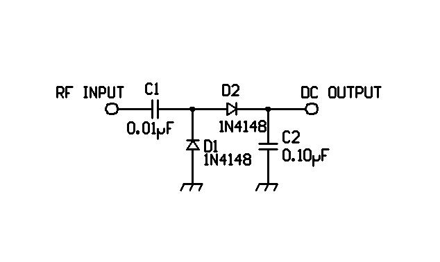
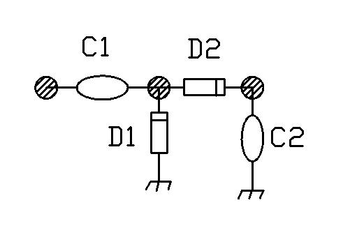
    The first thing to build is an RF probe. Go to the ARRL Handbook to page 26.9 and look at figure 26.9(C) for a voltage doubler circuit. Don't use the entire circuit. All you need is C1, C2, D1, and D2. The AC input will be the RF input and the point at which D1 and C2 meet will be the +DC output. Eliminate R1 and R2 from the circuit. The values here are not too critical and you can experiment with this. Use something like 0.1uF or smaller for C1 and something like 0.47uF or larger for C2. For D1 and D2, use the same diodes either Ge or Si. I used some surplus printed circuit board leaded diodes that I got surplus somewhere and of type 1N4148 or 1N914 silicon diodes.

    I won't go into the nitty-gritty details here, but you need three pads and just a small segment of printed circuit board. I have a photo of my finished probe below. Because the leads were short I mounted the diodes horizontally. D1 is between two pads and D2 is soldered to the center pad and the other lead soldered to the ground plane. You can with longer leads mount the diodes in a vertical position. The probe will work the same with either configuration. Build two and check it out if you want. I'll wait.

    photo 3 RF probe built Manhattan style.

    photo 3a RF probe schematic.

    photo 3b RF probe layout Manhattan style.

    I have a Ballantine RF probe that I purchased for $10 at a Livermore Swapmeet on a trip to CA when I was working. I happened to be in the San Jose area the weekend of the Livermore meet and the NorCal meeting. This probe came sealed in an aluminum pouch with all kinds of military part numbers, etc. Probably cost the tax payers a few hundred dollars. I compared my readings with the RF probe built Manhattan style and the Ballantine probe and got the same results to over 40MHz. The one shown in the photo probably cost me about a quarter. The commercial probe is nice, but not everyone can find such a great deal. Besides, in the building of HB gear you can take extra pride in using something that you personally built and can repair. Speaking of repair. You will be repairing this probe if you attempt to measure RF levels of several volts or more because the current levels through the diodes will exceed their limits and destroy them. Use this probe only for small signal level tracing. I tested the probe with an HP constant voltage generator from 100KHz to 100MHz and from about 1MHz to 50MHz the probes work well. The upper and lower frequency limits have some known issues, which I don't have room here to cover.

    Now since I am writing this article without knowing just how much your budget allows for test equipment and how much you already own and use I will assume that the audience is just starting out. I will show you in part 2 that with a DVM, and RF probe, and a crystal checker we can build a complete transceiver. You will need a general coverage receiver or a frequency counter later on. If you don't have a general coverage receiver or frequency counter, then you will need to own or be able to get access to a ham receiver on the band for which you are building.

    OK, let's now build a crystal checker. For this we will need a few more parts than before. You will need 39K and 1K 1/4W resistors. Capacitor values of 680pF, 150pF and 56pF in disk or mono and two 0.001uF caps and two diodes 1N4148 or 1N914 silicon or 1N270 in germanium. You will also need a 9V battery connector and a NPN transistor like the 2N2222 plastic transistor, meaning that the case is plastic. I use two pins from a machined Augut socket for connecting pins to hold the crystal under test. Here is the circuit diagram and the photo on my final wired circuit. Note just how small the circuit is doing the Manhattan construction vs. the printed circuit board. Note that I use two pin leads for the connecting points for the DVM and the frequency counter.

    This crystal tester is your basic Colpitts Oscillator with a voltage doubler. The output voltage from the voltage doubler can be used to get an idea of the crystal activity, i.e. just how well it resonants, with an increased voltage meaning high activity. I use this circuit with a frequency counter to match crystals for IF filters. It works well and it is very cheap to build.

    photo 1 Crystal checker built Manhattan style.

    photo 1a Crystal checker layout Manhattan style.

    I use this critter quite frequently for testing unmarked crystals and crystals in kits to match them more closely. You will find it quite handy. Because it comes out so small (and you don't have to make yours look just like mine) I have to take care in putting it up somewhere so that it doesn't get lost in the clutter on the workbench.

    Here is a photo of a similar crystal checker from the G-QRP club kit and the HB Manhattan style crystal checker. You can see how much less room a circuit will occupy with this technique.

    photo 2 Crystal checker from G3RJV and the Manhattan one.


    Final Housing for Projects

    In this section I will talk about how I install final projects in homebrew cases.

    There are many ways in which to house a final project if you so chose. I will not even attempt to start describing all of the ways, but choose to discuss the making of aluminum shells similar to those manufactured by TenTec and others. George Heron, N2APB, will have an article in this issue on building using printed circuit board material and it is a good way to go also.

    What I do is make two u-shaped shell from 0.040" aluminum sheet. I make a paper pattern for each half of the enclosure and tape them to the aluminum sheet. Then using the shear I cut the two rectangular pieces to size, usually from a single sheet of aluminum. I then take a file and smooth all the edges.

    And then taking the brake portion of the Harbor Freight combo, I very carefully make 90 degree bends along the lines that I have drawn on the plan and then make sure that the two pieces match. So far I have been lucky and haven't made any mistake whereby I had to redo one of the halves. If you do, save the "bad" one for use later in another project and you only have to make the matching half.

    Once you have the two halves you need to make an L-shaped piece that is used to hold the two halves together. I use brass stock that I buy at the hobby shop. I cut and bend using the shear and brake to make a small L-shaped piece. You can then use a tap to make threads for the size screws that will hold this piece to the bottom half of the case and the screw that will hold the top half in place and also allow you to remove it for whatever reason.

    Then you drill the holes in front and back of the case for the connectors and controls after carefully measuring and marking for each. You could do this before you bend the aluminum and be able to use a drill press to due careful work. Carefully sand both halves and then clean with any cleaner you choose to eliminate finger prints and dirt and grime from the surface. Now I personally choose not to prime the surface. I have been using some paint from Wal-Mart that costs $0.98 for the regular and $1.49 or so for the satin finish. The brand name on the paint is ColorPlace and it is an indoor/outdoor paint. I like the results of the satin finish in the royal blue color. The TT2/MRX transmitter-receiver combo that I won first place at Pacificon with was painted with only one coat of the paint. Otherwise, I'd have been drying the paint on the trip!! I was that close to the deadline on the project.

    I use press-on lettering from the hobby shop to label the controls. If you put a clear coat of Krylon or other paint be warned that the paint will most likely attack the lettering and cause it to wrinkle. Go gently and get advice from others on just how to do this. I'm still experimenting on this one. If you do not place a clear coat over the lettering then over a period of time and use the lettering will wear off the case. The coating of clear is to protect the letters.

    Here are a couple of photographs of the rig. Note that I have yet to do the bracket as it hasn't been together long enough and I use it for show and tell a lot. Also note that the circuit board is just attached to the lower half-shell with contact cement. I use Design Master Tack 1000 Spray Adhesive that I bought at Ben Franklin Crafts' Store for $4.99. It will hold down the board and it is not permanent, i.e. I can peel the board up with no damage. Haven't tried it but I followed the instructions on the can. You may choose to use screws or standoffs to mount the board to the case. By directly attaching the board to the base I lower the overall height of the case and reduce the size of the final assembly.

    TT2/MRX Combo Tuna Tin 2 and MRX receiver from NorCal contest that were built Manhattan style on same board with K7QO final PA Cheby filter and W7ZOI keying circuit. Also note homebrew K7QO case with 040 Al and use of Harbor Freight shear.

    TT2/MRX Combo Same as previous photo with different view.


    The Future Paths Possible

    Now, with the basics covered as best I could with resource limits of time and space, I hope that I have given you some insight on building using this technique called Manhattan Style construction. You can build any number of projects using the technique of your choice. It is not the intent here to put Manhattan building above any of the others. We each enjoy using what we think suits us best and that is the whole game plan.

    I would like to see you research through the ARRL Handbook and your library and collection of designs, schematics, and projects in progress and find some simple things to build between now and the next issue of this newsletter. I would recommend you go through the test equipment sections of the Handbook and Wes Hayward's, W7ZOI, "Solid State Design for the Radio Amateur". You now have the ability to build anything that you want. Bring all your stuff to the gatherings of other QRPers. It will motivate them to do more and we all want to see your work. It's the only way for each of us to learn new things.

    My plans are to take the NN1G rig and redo it for 17 meters. I will build it and then in the next issue write a complete article on everything that I did and why I did it. I have been permission by Dave Benson, NN1G, to use the schematics and I include the 20 meter version here to "prime the pump" so to speak. Study the schematic and determine what each section does. I have taken the VFO section and replaced it with the new one from Dave's SWL series because the old one used an air variable which take up too much room and are difficult to find and more expensive than the varactor tuned VFO. I have not listed the individual parts in order to hold you off on even thinking about the 20 meter version and building it. Hey, there are plenty of rigs on 20 meters already. Let's sneak off to one of the WARC bands and play. OK? I ask that you do hold off on asking me where I am on the project via email, etc. so that I can get it done as best I can before the next deadline that George will put on me.

    So until the next time we meet may all your projects work the first time and everytime. 73 es dit dit.

    NN1G Mark II Schematic for 20 meters.


    References

    1. The American Radio Relay League, Inc., "The ARRL Handbook". Connecticut, The ARRL. 1995 and later.

    2. The American Radio Relay League, Inc., "QRP Classics". Connecticut, The ARRL. 1990.

    3. Doug DeMaw, W1FB, "Quick-and-Easy Circuit Boards for the Beginner". Connecticut, The ARRL. "QST" September 1979, page 30.

    4. Doug DeMaw, W1FB, "Experimenting for the Beginner". Connecticut, The ARRL. "QST" September 1981, page 11.

    5. Wayne Burdick, N6KR, "2N2222 Design Contest". QRP-L posting of

    6. Jim Kortge, K8IQY, http://www.qsl.net/k8iqy. Web page with information on the K8IQY rigs.

    7. Dan's Small Parts web page, http://www.fix.net/~jparker/dans.html

    8. Harbor Freight Tools Inc. web page, http://www.harborfreight.com/

    9. Almost All Electronics web page, http://www.aade.com/

    10. QRP Amateur Radio Club International, http://www.qrparci.org/

    11. QRPp Winter 1998, NorCal QRP Club. Yearly reprints available from Doug Hendrick, KI6DS, 862 Frank Ave, Dos Palos, CA 93620 for $15 up to and including 1997 and $20 per year thereafter. $4 shipping for 1 year and $5 for 2-3 years and $7 for 4-6 years. Make check or MO out to Doug not NorCal.


    The following are photos done with 35mm camera and then scanned in. The original photos are much better as I am learning here how to do this. George. Pick the ones you want me to send to you with the NN1G schematic.

    photo 1 Crystal checker built Manhattan style.

    photo 2 Crystal checker from G3RJV and the Manhattan one.

    photo 3 RF probe built Manhattan style.

    photo 4 Tuna Tin 2 and MRX receiver from NorCal contest that were built Manhattan style on same board with K7QO final PA Cheby filter and W7ZOI keying circuit. Also note homebrew K7QO case with 040 Al and use of Harbor Freight shear.

    photo 5 Same as photo 4 with different view.

    photo 6 Desert Ratt 3 regen receiver in K7QO HB case.

    photo 7 Desert Ratt 3 regen receiver in K7QO HB case.

    photo 8 K7QO test jig for AADE meter.

    photo 9 K7QO test jig with 0.10uF cap being measured.

    photo 10 Tools used for Manhattan building. Clockwise direction --- Harbor Freight tweezers, Al sanding block, R/S solder stand, Kester solder, Weller soldering iron with Ungar tip, chain nose pliars, Exacto hobby knife with #11 blade, and Sears diagonal cutters.

    photo 11 Another TT2 photo.

    photo 12 Crystal checker and RF probe together.

    NN1G Schematic in .pdf format