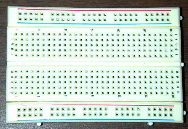
Jameco JE21 breadboard (actual size 2.1 by 3.2 inches)
by Lyle Koehler, K0LR
Introduction
This article describes how to use solderless breadboards, which can overcome some of the problems of dealing with today's tiny components, and which provide a quick and easy way to build or modify home brewed circuits. I will start with a description of what solderless breadboards are, and then provide construction details and/or schematics for sample projects that lend themselves well to solderless breadboarding. More projects will be added in the future.
Solderless breadboards are great tools for the experimenter. They provide the closest thing to instant gratification that you are likely to find in electronic circuit construction. Component leads are plugged directly into holes in the board, where spring clips make electrical connection to the leads and also hold the components in place. The boards come in a variety of sizes, from about 2 by 3 inches up to 7.5 by 7.5 inches. The smallest boards will hold up to four 14 pin dual inline packages (also called DIPs), and the larger boards can hold 30 or more DIP integrated circuits. The holes in the board will accomodate wire sizes between number 20 and number 28, corresponding to diameters between 32 thousandths of an inch and 13 thousandths of an inch. It takes about a quarter of an inch of bare lead inserted into the hole to make electrical contact. If a component has leads that are too big, too small or too short, I simply solder pieces of the proper size wire to the leads. I know, the boards are supposed to be solderless, but you can't have everything. Excess leads clipped from resistors and capacitors used on previous projects work well for this purpose, as well as when you need short jumpers between points on the board. Larger boards come with plastic or aluminum back plates and with two or more binding posts for attaching wires from external circuits. Of course, you can attach a wire of the correct size to any hole in the breadboard, but they will pull out if you put too much strain on them.
It may seem that solderless breadboards are not suitable for RF applications, or that with so many spring contact connections, they must be unreliable. I wouldn't use one for a high performance VHF rig, or for the life support system in a manned space vehicle. However, they work pretty well through the HF range, and at least for simple circuits, contact failure is not likely to be a problem. Most of the circuits and subcircuits used in my homebrew construction projects are first checked out by building them on a solderless breadboard. There is nothing to stop you from putting a finished solderless circuit in a box and using it as a "permanent" piece of equipment, as I have done on more than one occasion.
Solderless breadboards vary in price depending on size, brand, and where you buy them. The largest one available in Radio Shack stores normally costs about $22, but I've seen them on sale at www.RadioShack.com for about $12.50, and vendors like Jameco Electronics have similar boards for about the same price. Jameco's largest board costs about $31, while the same size board in other brands or from other vendors can cost 65 dollars or more. Boards are also available as part of experimenter stations with built in power supplies and a variety of other "bells and whistles" at prices of several hundred dollars.
The description that follows is for a generic, small solderless prototyping board like the Jameco JE21 (about $5 each) shown in the photograph below. Larger boards use the same basic layout except that they are longer, and two, three or four of them are stacked side by side. Just above the bottom of the board there are two lengthwise rows of holes. Actually the rows of holes aren't continuous; for some reason they are arranged in groups of five with a gap between each group. However, the holes in each lengthwise row are connected together inside the breadboard, so that they can be used for connections such as power and ground that are shared with many components in your circuit. Later on, I may refer to these lengthwise rows of holes as the bus strips, or the power and ground buses. On longer boards, the bus strips are often split in the middle so that they can be used for different connections on the left and right halves of the board. I usually find this more of a confusion factor than a benefit, so I run jumpers across the gaps as soon as I start a project. Sometimes I forget, and wonder why there is no power or a bad ground connection to some of the components. There is usually no marking to tell you that the left and right halves of the bus are not connected, except that there is a larger gap between the middle groups of five holes than the others. Jumper wires must be installed across the gap if you want the same bus to run the entire length of the board.
Jameco JE21 breadboard (actual size 2.1 by 3.2 inches)
Above the bottom two rows of holes, which make up the bus strips, there is a gap, and above that there are 5 rows of holes on a uniform 0.1 inch grid spacing, running the entire length of the board. However, instead of being connected internally in a lengthwise direction like the bus strips, these holes are connected together vertically in groups of 5. Suppose we plug an integrated circuit (we will shorten that to IC) into the breadboard so that it straddles the big groove in the middle. The spacing of the holes is arranged so that the leads on a standard 14 or 16 pin IC package will fit into the first holes on each side of the middle groove. Since the holes are connected together in groups of five, that leaves 4 available points to connect other components to each pin on the IC. What if more than four things need to be connected to one IC pin? You run a jumper wire to an unused group of holes somewhere else on the board and expand from there.
As mentioned earlier, the board is symmetrical, and the same patterns we have already described are repeated above the middle groove. To summarize the board description, starting from the top there are two lengthwise rows of holes connected together internally (but the two rows are insulated from each other). Then there is a gap of smooth plastic. Below that, there are 5 lengthwise rows of holes that are connected together vertically in groups of 5 (but every group of 5 vertical holes is insulated from all other groups). Then we come to the large middle groove, 5 more rows of holes, a gap, and finally two more rows before the bottom of the board. If you have an ohmmeter or audible continuity checker, it might help to connect a couple of small wires to the test probes and literally poke around in the board, getting familiar with its internal connection pattern.
There is no special trick to inserting component leads or jumper wires into the board. However, the ends of the leads must be clean, smooth, bare and straight for at least one quarter inch. You also need to make sure that the wire is inserted straight down into the hole; that is, perpendicular to the board surface. Sometimes a component lead or the hole will be stubborn; in that case make sure the lead is straight and without any burrs on the end. I often have to squeeze the leads gently in the jaws of a needle-nose pliers to remove any little kinks, especially on used components from my junkbox. It helps to grab the lead just above the insertion point with a tweezers or needle nose pliers so that it has less room to bend as you try to push it into the hole. It is important for RF circuits to keep leads as short as practical (not necessarily as short as possible). Keeping them short also reduces the chances of two bare component leads touching each other. For most small components and short jumper wires, I try to bend the leads to fit the desired hole spacing, and then insert both leads at the same time. This usually works better than leaving the wires long enough so that you can insert one end first and then the other. But whatever works for you, as they say. Often you have no choice in the matter, as is the case with integrated circuits where you have to insert 14, 16 or more pins essentially all at the same time.
Integrated circuits usually come with their leads spread out slightly, so that you have to bend them inward a bit to make them fit the hole pattern. The same thing is true when you try to put an IC into a socket or insert it into a conventional soldered circuit board. If necessary, I bend the pins by grabbing the IC firmly by the ends (I have small fingers; it might be harder for other people). Then I hold the IC so that the top of the plastic case is vertical and push the leads down gently against a horizontal flat surface. The idea is to get the leads to line up perpendicular to the top of the IC package, with the leads on each side parallel to each other. 14 or 16 pin ICs are not too hard to insert. Usually this bending operation is not necessary on breadboards; you can take the ICs just the way they come from the supplier and use your fingers to encourage the pins to go into the holes in the board, but you do have to be careful not to mash any of the pins. It gets tougher with 28 or 40 pin ICs; fortunately I don't deal with them very often. Once an IC has been inserted correctly in a breadboard or IC socket, the pins are pretty well aligned and it is easy to remove and re-use them. That's one beauty of the solderless breadboard. If you don't like the way the circuit works or simply get tired of it, you can pull out the parts and use them to build something else.
Notes on using the bus strips at the top and bottom of the board: I usually use the inner bus strip (the upper one) at the bottom of the board for the ground bus, and the inner strip at the top of the board for power. This helps me build a circuit from a schematic, because schematics tend to show the power connections at the top and the ground connections at the bottom. However, quite often you will want to connect a lead on the top of the board to the ground bus, or a component on the bottom of the board to the power bus. If you don't need the remaining two bus strips for any other connections, connect the outer bus on the top to ground and the outer bus on the bottom to power, so that both buses are available on each side of center. An example of a larger breadboard with the power and ground buses connected in this way is given in the photograph below. Note that this breadboard has two vertical bus strips on either end of the board. I have connected one set of the vertical strips to two of the binding posts and used them to distribute the power and ground connections to the horizontal buses. Also note the orange jumpers that bridge the gaps in the middle of the horizontal bus strips.
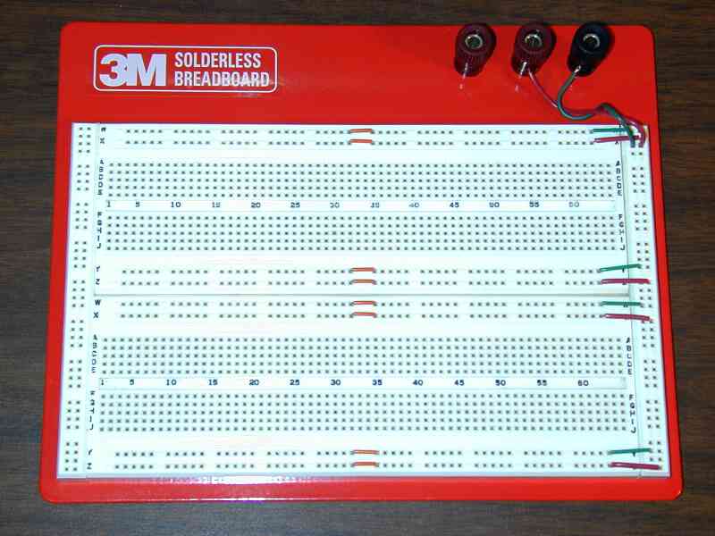
3M Solderless Breadboard with power and ground jumpers installed
Many suppliers of solderless breadboards also sell pre-cut jumper wires in various sizes. Somehow they never seem to be the right size, so I find it more effective to make my own. I have often made jumpers from the insulated #26 solid copper wire found in multi-conductor telephone cables. However, the #26 wire is just a little bit flimsy, and something like #22 or #24 is better. Radio Shack sells a three-roll set (three colors) of #22 insulated solid wire as catalog number 278-1221. Bare tinned bus wire is also good for jumpers, as long as they are very short and in locations where there is a low risk of the bare leads touching each other. When trimming excess lead lengths from components such as resistors and capacitors, I often save the pieces of bare tinned wire and use them for short jumpers.
Various techniques can be used for connections to the outside world and to circuit components like switches, connectors and potentiometers. Since most of these off-board components are fairly easy to work with, soldering one end of a jumper wire to the component should not present a problem. Another option is to use a clip lead for the connection to the component, with the other end of the clip lead attached to a short bare wire that is plugged into the breadboard. To provide a somewhat stronger connection, it helps to bend the bare wire into a U shape and plug it into two holes in the breadboard; then connect the clip lead to the exposed center of the U. Other techniques like crimp connectors, screw terminals, wire nuts, etc. can be used if you really have an aversion to soldering. On larger solderless breadboards with backplanes and binding posts, you can attach leads to the binding posts and/or drill additional holes in the protruding portion of the backplane to mount connectors, switches, etc. A metal L shaped bracket, attached to the bottom of the breadboard with double sticky tape, can serve as a mounting point for external connections and a temporary (or permanent) front panel for your project.
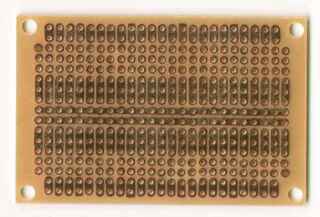 What if you
want to re-build your project in more permanent form, but don't want to
go to the trouble of laying out a PC board? I have seen pre-etched and
pre-drilled project boards that have the same hole layout as solderless
breadboards, so that the project can be transferred directly. Being too
cheap to buy those exotic boards, I normally use the little project boards
from Radio Shack like the one shown on the left. Its layout is similar
to the solderless breadboard except that there are fewer connection points,
and the buses used for power and ground run down the middle of the board
rather than along the outside edges.
What if you
want to re-build your project in more permanent form, but don't want to
go to the trouble of laying out a PC board? I have seen pre-etched and
pre-drilled project boards that have the same hole layout as solderless
breadboards, so that the project can be transferred directly. Being too
cheap to buy those exotic boards, I normally use the little project boards
from Radio Shack like the one shown on the left. Its layout is similar
to the solderless breadboard except that there are fewer connection points,
and the buses used for power and ground run down the middle of the board
rather than along the outside edges.
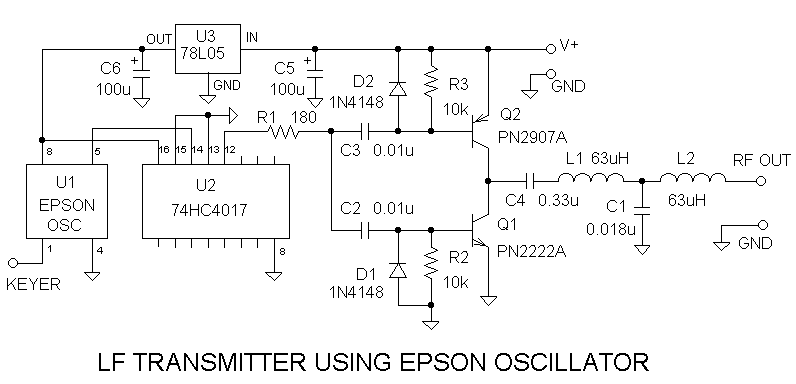
The LowFER transmitter described in this article is shown built on a Jameco JE21 solderless breadboard that is about 3.2 inches long and 2.1 inches wide (a larger breadboard will also work, of course). This transmitter circuit is similar to the "Simple LowFER Transmitter" described elsewhere on my web page, but it uses an Epson programmable crystal oscillator module. The Epson module offers an inexpensive way to get a custom crystal AND the oscillator circuit all in one compact package. These oscillators are a little noisy for use in HF circuits, but when divided down to the LF region, the phase noise is very low. In this circuit, an oscillator operating at approximately 1.8 MHz is divided down by a factor of 10 in a 74HC4017 integrated circuit, which in turn drives a complementary pair final amplifier. The final amplifier will handle the 1 watt FCC Part 15 power limit for operation in the 160 to 190 kHz region, and will provide an efficiency in excess of 80 per cent when driving a 50 ohm resistive load.
A completed breadboard transmitter is shown in the photograph below. The Epson oscillator module is in the mini-DIP package at the left of the protoboard. It oscillates at its specified frequency of 1.8373 MHz, and I marked it with a piece of tape so that it wouldn't get mixed up with other Epson modules in my collection. The oscillator module has four pins: power, ground, output, and output enable. In this photograph, nothing is connected to pin 1, the output enable pin. It has a high-resistance internal pullup, so that the output is enabled as long as pin 1 is left open, and disabled when pin 1 is pulled to ground through an external circuit. To key this transmitter, I would connect a 10k protection resistor between pin 1 and an external keyer such as the PC beacon identifier described elsewhere on my web site. Note, however, that a conventional ham keyer that pulls a keying line to ground for the "key-down" condition will require an inverting circuit. Some keyers (including the PC beacon keyer) offer the option of "normal" or "inverted" keying. If you simply want to try the transmitter with a good old fashioned straight key, connect a 10k resistor from pin 1 of the oscillator to ground, and connect the straight key between pin 1 and +5 volts (pin 8 on the oscillator package -- pins 2,3,6 and 7 do not exist).
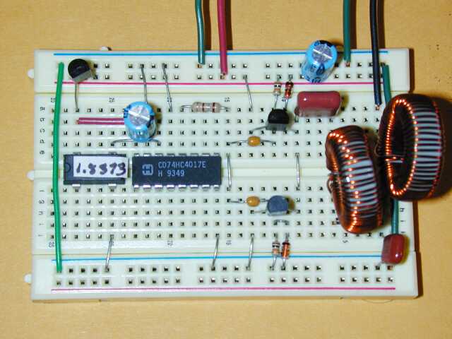
The oscillator feeds a 74HC4017 divide by 10 circuit, and the output of the divider (in this case, at 183.73 kHz) drives a complementary pair final. Same final circuit and lowpass output filter as used in my "Simple LowFER Transmitter" and in the synthesized LF transmitter with built-in keyer. The only other parts on the circuit board are a 78L05 regulator in the upper left, and two electrolytic bypass capacitors.
It is almost possible to build the circuit from the photograph, but a few of the connection points are hidden beneath components. The diagram below shows all of the connections. Bus strips on the solderless breadboard are indicated by grey lines; jumper wires are shown in red, and component outlines are in pale blue. Connection points (where jumper wires or component leads are inserted into the board) are shown as black circles.
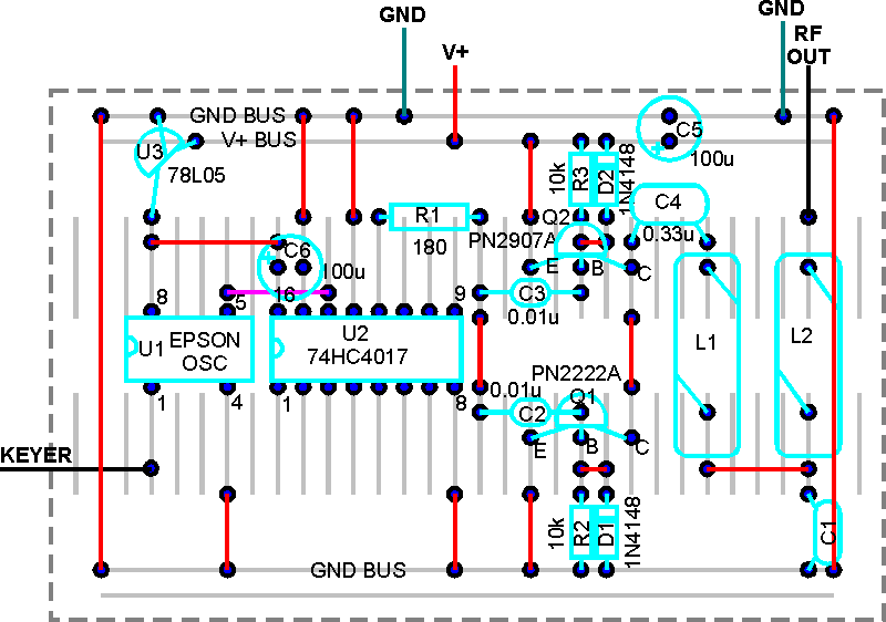
SOLDERLESS BREADBOARD LAYOUT
Some of us need a schematic to see what the circuit really looks like, so I have included one below. Values for L1, L2 and C1 are for a 50 ohm load. L1 and L2 are made with 60 turns of #26 or #24 AWG wire on T-80-3 toroid cores. To see the values for other load resistances, and to find the number of turns required on the toroid coil forms, please refer to the article on the synthesized LowFER transmitter with built-in keyer.
Parts list for LF transmitter:
C1: 0.018 uF capacitor -- Digi-Key # EF1183
C2, C3: 0.01 uF capacitor -- Digi-Key # P4963
C4: 0.33 uF capacitor -- Digi-Key # EF1334
C5, C6: 100 uF 25V capacitor -- Digi-Key # P5152
D1, D2: 1N4148 diode -- RadioShack.com # 900-2908
L1, L2: Toroid inductors (see text) -- RadioShack.com # 900-7027 (package of 3)
Q1: PN2222A transistor -- RadioShack.com # 900-5420
Q2: PN2907A transistor -- RadioShack.com # 900-5421
R1: 180 ohm resistor -- Digi-Key # 180EBK (package of 5)
R2, R3: 10k resistor -- Digi-Key # 10KEBK (package of 5)
U1: Epson programmable oscillator -- Digi-Key # SG-8002DC-PHB (specify a frequency that is 10 times the desired transmit frequency)
U2: 74HC4017 HCMOS divider -- Jameco # 45891 or RadioShack.com # 900-3515
U3: 78L05 low power 5V regulator -- Jameco # 51182 or RadioShack.com # 900-4491
Solderless breadboard: Jameco catalog # 20600 or larger Digi-Key # 923252. (RadioShack.com # 910-1262 is also a larger board, and comes with a backplane and binding posts.)
You will also need jumper wires and a small quantity of #24 or #26 enamel insulated magnet wire; about 55 inches for each toroid inductor. Radio Shack stores carry a set of three spools of magnet wire (#22, #26 and #30); their catalog number is 278-1345. Links to Digi-Key, RadioShack.com and Jameco are given below.
For most people, the hardest, or at least the most tedious part of constructing a circuit like this, is winding the toroid inductors. Many would-be home brewers may have fainted or turned off their computers when they saw the toroid coils in the picture of the completed transmitter. However, if you have read this far, it means that you survived the initial shock and should be able to master the incredibly difficult task of stringing a 0.025 inch wire through a 0.5 inch hole. Either #24 or #26 wire can be used for L1 and L2. The losses might be a tiny bit lower with #24 wire, although the difference in output would be difficult to measure. It is easier to work with #26, and the choice is up to the builder (in other words, use whatever is in your junkbox). If you pull each turn fairly tight on the form, it takes about 7/8 inch of wire per turn on a T80-3 form. Allowing an extra inch or so on each end, I would cut the wire to an initial length of about 55 inches for the 60 turn coil used in the 50 ohm version of the filter. Winding the coils may be a little easier if you find the mid-point of the wire and wind from the center toward each end. That method doesnt require pulling the entire length of wire through the core at the beginning of the winding process. One advantage of using #24 wire is that 60 turns (close wound, single layer) will fill up the form. If you lose count of turns, as I always do, just keep winding until the core is full, or until you run out of wire, and call it 60 turns. Make sure that you scrape the enamel insulation from the ends of the windings on L1 and L2 so that they will make contact with the solderless breadboard.
To test the circuit, connect a 50 ohm resistor across the output and apply about 12 volts DC to the V+ bus. With the oscillator enabled (pin 1 open circuited or pulled to +5 volts), tune your receiver to the oscillator frequency (which is 1.8373 MHz in my prototype transmitter) and to the oscillator frequency divided by 10. You should be able to hear strong signals at both frequencies. If necessary, connect a short indoor antenna consisting of a few feet of wire to the receiver and bring the wire close to the breadboard. After the transmitter has been running for a short time, the 50 ohm load resistor will be quite hot to the touch, but transistors Q1 and Q2 should not get warm if things are working properly. By the way, Q1 and Q2 will get warm if the transmitter output is not connected to a proper load, which includes having a transmitting antenna that is not tuned to resonance. To determine the final amplifier current, you can remove the jumper going from the V+ bus to the emitter of Q2. This will disconnect the final amplifier so that you can measure the current used by the oscillator and divider alone. Then reconnect the jumper, measure the total current, and subtract the value of current measured in the first step. The remainder is the final current. With a 50 ohm resistive load, the power input to the final will typically be 1 watt when V+ is about 14 volts.
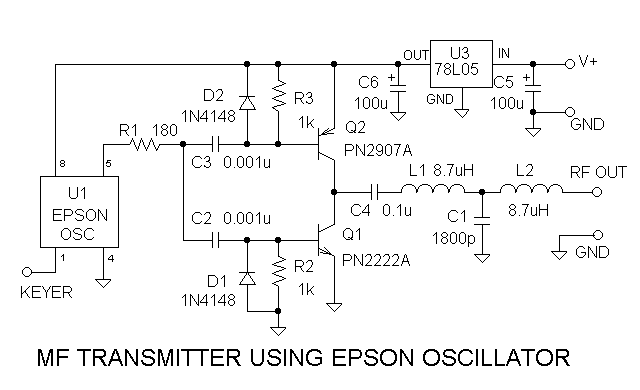
With a few modifications, the same basic circuit as the LF transmitter can also be used in the 1.6 to 1.705 MHz range. The circuit is simplified because the Epson oscillators are available for direct operation at this frequency, and it is not necessary to use a divide by 10 stage. The circuit diagram for the MF transmitter is shown below. L1 and L2 are wound with 42 turns of #26 wire on T50-2 (red) cores. Note that the entire circuit, including the final amplifier, operates from 5 volts DC. A 78L05 regulator is shown in the schematic so that the transmitter can be operated from supplies in the 9 to 15 volt DC range. If you already have a regulated 5 volt supply, there is of course no need for the regulator. I did not include a picture or board layout, because I haven't actually built this exact circuit. However, the final amplifier is the same design used for several years on my "MIN" MedFER beacon before the expanded AM broadcast band became populated with stations. Board layout for the final amplifier can be identical to that of the LF version.
Parts list for MF transmitter:
C1: 1800 pF capacitor -- Digi-Key # PCC182BCC
C2, C3: 0.001 uF capacitor -- Digi-Key # P4898
C4: 0.1 uF capacitor -- Digi-Key # P4924
C5, C6: 100 uF 25V capacitor -- Digi-Key # P5152
D1, D2: 1N4148 diode -- RadioShack.com # 900-2908
L1, L2: Toroid inductors (see text) -- RadioShack.com # 900-7015 (package of 4)
Q1: PN2222A transistor -- RadioShack.com # 900-5420
Q2: PN2907A transistor -- RadioShack.com # 900-5421
R1: 180 ohm resistor -- Digi-Key # 180EBK (package of 5)
R2, R3: 1k resistor -- Digi-Key # 1.0KEBK (package of 5)
U1: Epson programmable oscillator -- Digi-Key # SG-8002DC-PHB (specify the desired transmit frequency)
U3: 78L05 low power 5V regulator -- Jameco # 51182 or RadioShack.com # 900-4491
This parts list is included for the convenience of the builder. The same value parts from other suppliers or from your junkbox will work equally well. You'll also need some #26 enamel insulated "magnet" wire to wind L1 and L2; approximately 3 feet of wire for each inductor.
Before proceeding, let's look at the advantages and disadvantages of an LF converter (or upconverter, as it's sometimes called) as opposed to a preamp. If your receiver already tunes the entire frequency range that you are interested in, a preamp is probably the way to go. With a converter, the overall frequency accuracy and stability depends on the local oscillator in the converter as well as the stability of the receiver itself. Stability and accuracy in most receivers is directly related to frequency. For example, at the moment the reference oscillator in my IC-706 is off by about 0.5 ppm. At 200 kHz, that's an error of only 0.1 Hz, but at 14 MHz the error would be 7 Hz. Not a problem for normal listening, but unacceptable for modes like coherent BPSK. And the IC-706 has a very good reference oscillator even by modern receiver standards. The oscillator in the converter is likely to have much poorer stability than the reference oscillator in the receiver. So why use a converter at all? For one thing, most receivers are very insensitive on LF, and it helps to convert the signal up into the HF range where the receiver's performance is optimized. But that is simply a matter of gain, and could be accomplished with a preamp. The primary reason for a converter is to extend the frequency coverage beyond what the receiver will normally tune. With this converter, you'll be able to hear signals from a few kHz up to 500 kHz or more.
A sensitive LF converter using the popular NE602 oscillator/mixer IC is shown below in protoboard form. Unfortunately the NE602 can be overloaded fairly easily by strong signals, so a tuned input circuit is used to provide a sharp peak in the LF range and reject signals in the AM broadcast band. The peak can be tuned from about 150 kHz to 400 kHz. For lower frequencies, a larger inductor and/or fixed capacitors in parallel with the air variable can be used to lower the frequency response. However, the input circuit does not roll off very steeply at frequencies below 150 kHz, and with even a modest length of wire antenna it is possible to hear signals between 10 and 100 kHz without making any changes to the input components.
LF converter with air variable tuning capacitor
As can be seen from the photograph, the 365 pF air variable capacitor used to tune the input is almost as large as the solderless breadboard that contains the rest of the circuit. Note that neither the rotor or the stator of the air variable capacitor is grounded in this circuit, so if the finished converter is housed in a metal box, insulating screws and washers must be used to mount the capacitor, and clearance must be allowed between the capacitor shaft and the front panel. The schematic diagram for the circuit is shown below. Input peaking is provided by the series combination of the air variable capacitor C3 and a fixed inductor L1. Capacitor C2 is connected across the input of the NE602, to provide a low impedance to ground for frequencies above the LF range. C2 also acts as an impedance transformer so that the input resistance of the NE602 does not load the tuned circuit excessively and decrease the Q. Capacitor C1 also helps to limit the high frequency response of the input circuit, and insures that C3 and L1 can be tuned to resonance even if a high impedance antenna such as a fairly short length of wire is connected to the input. The output impedance of the NE602 is about 1.5k ohms, which is a pretty poor match to the 50 ohm input of most receivers. Transistor Q1 is connected as an emitter follower circuit to improve the impedance match, and this increases the overall gain. Q1 gets its bias from the voltage drop that exists between the power pin of the NE602 (pin 8) and the output pin (pin 4). Pin 2 of the NE602, an unused input, is bypassed to ground through C4, while the unused output at pin 5 is left unconnected.
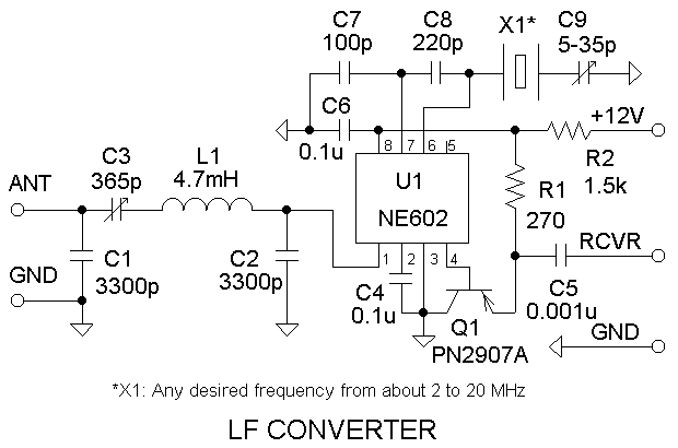
Capacitors C7 and C8 along with crystal X1 form a Colpitts oscillator circuit, and trimmer capacitor C9 is used to fine-tune the crystal oscillator to the desired frequency. In some cases it isn't important to trim the oscillator frequency. For example, I use Icom receivers which have a receiver incremental tuning (RIT) control that will offset the receive frequency without changing the frequency display on the receiver (Kenwoods don't work that way). With that kind of receiver, you can replace trimmer C9 with a fixed capacitor of about 20 to 30 pF, or simply put a jumper wire to ground in place of C9, and use the RIT control to correct for any frequency offset. I haven't tested this circuit with every type of crystal, but the inexpensive metal-can "microprocessor" crystals are almost sure to work. Almost any crystal frequency from 2 MHz to 20 MHz can be used. The choice of local oscillator frequency for the converter depends primarily on your receiver. If the receiver is general coverage, almost any multiple of 1 MHz is OK. The reason for using an integer multiple of 1 MHz is to simplify the mental math in figuring out the actual LF input frequency. For example, if I want to receive 187 kHz with a 4-MHz local oscillator in the converter, I simply tune the receiver to 4.187 MHz. If the converter is to be used with a ham-band only receiver, a crystal frequency such as 7.000 or 14.000 MHz would be preferred. A lower frequency is better from the standpoint of stability, as discussed earlier. There is another consideration in choosing a local oscillator frequency. Very strong HF signals will "bleed through" the converter, so you should avoid converter output frequencies that have a lot of shortwave broadcasting or ham activity if possible. I use 4 MHz crystals because they are cheap, readily available, and there aren't many broadcast stations or other strong signal sources in the 4.0 to 4.5 MHz range (corresponding to 0 to 500 kHz converter input frequencies).
The NE602 is designed for supply voltages between 4.5 and 8.0 volts, and the absolute maximum rating is 9 volts. Resistor R2 is shown in the circuit as 1.5k, which is about right for use with a 12 volt supply. The whole circuit draws about 4 mA, so that the drop across a 1.5k resistor is nominally 6 volts. A resistance of 1k or less would be used for operation from a 9 volt battery, and no series resistance is needed if you operate the converter from a 6 volt supply.
Component locations are shown in the close-up of the breadboard. Capacitor C3 is located off the board, and only the wire leads are visible. I didn't draw up a detailed manual layout because it's very time consuming, and between the picture and the schematic it shouldn't be too hard to figure things out for yourself. Then too, some changes in the layout may be necessary depending on how closely the shape and size of the components you use match the ones I grabbed from my junkbox. For the input and output connections, I used pieces of RG-174 coax with bare solid wires soldered to the ends that plug into the board, and RCA phono jacks on the other ends. You can see the coax connections to the board, but the RCA jacks are not visible in the picture.
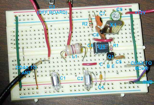
Component locations for LF converter
I recommend a coax-fed wire antenna, maybe 30 feet long and as high as possible. Longer wires will give more signal, along with more noise, and more chance for overload. An 80 or 40 meter dipole should work fine, as long as it does not have a transformer-type balun (choke baluns or coiled coax baluns are fine, but transformer baluns typically attenuate the heck out of LF signals). I can hear local LowFERs BK, RM, BRO, and lots of NDBs on a 20 meter dipole fed with about 125 feet of coax. WWVB at 60 kHz and the strong Navy RTTY signals in the 24 kHz range should boom in on almost any outdoor wire antenna. If you want to try a multi-turn receiving loop, I recommend connecting it in series between C3 and L1. Remember, though, that the capacitance of any coax cable you use between the loop (about 30 pF per foot for 50 ohm coax) will be in shunt with the loop, so keep the cable as short as possible.
To check out the converter, connect the output to your receiver, apply power and tune the receiver around the vicinity of the crystal oscillator frequency. You should hear a big signal if the circuit is working. Adjust C9 until the oscillator signal is on the correct frequency according to your receiver. Because the oscillator signal is so strong, it may be better to use an actual off-the-air signal for final tweaking. I use WWVB at 60 kHz because it puts in a good signal night and day, and is a very precise reference. NDBs are not necessarily good calibration sources if you want extreme accuracy; they can easily be off by 20 Hz. In case you have never heard WWVB before, it does not have any voice modulation. The signal is keyed by a time code similar to the low-pitched audio tones that you hear in the background during part of the WWV HF transmission cycle. WWVB's modulation does not turn the carrier completely on and off; instead the carrier amplitude is varied by 10 dB. Listening in CW mode on a receiver with good AGC, it may be difficult to hear the changes in signal amplitude. However, it will show up on the S meter, and is easier to detect with the AGC off or the RF gain turned down. The best description of WWVB's modulation is that it sounds like somebody sending slow CW with a sloppy fist.
Parts list for the LF converter:
C1, C2: 3300 pF capacitor, Mouser No. 23PS233
C3: Air variable capacitor, 365 pF or greater (see notes)
C4, C6: 0.1 uF capacitor, Mouser # 147-72-104
C5: 0.001 uF capacitor, Mouser # 140-50P2-102K
C7: 100 pF capacitor, Mouser # 140-50N5-101J
C8: 220 pF capacitor, Mouser # 140-50N5-221J
C9: 9-50 pF trimmer capacitor, Mouser # 24AA024
L1: 4.7 millihenry inductor, Mouser # 434-06-472J
Q1: PN2907A transistor, Mouser # 610-PN2907A
R1: 270 ohm resistor, Mouser # 30BJ250-270
R2: 1500 ohm resistor, Mouser # 30BJ250-1.5k
U1: NE602AN, NE612AN, SA602AN or SA612AN integrated circuit (see notes)
X1: Crystal for desired frequency, such as 4.00 MHz Mouser # 559-FOX040
Notes on parts for the LF converter:
Mouser Electronics is on the web at http://www.mouser.com There are no really critical parts in the circuit; feel free to substitute what you have in your junk box or any equivalent parts from your favorite supplier. Two items may be difficult to find. Air variable capacitors are becoming scarcer and more expensive; one of these days I expect to start seeing them on "Antiques Roadshow". If you can't find one at a swap meet, a good source for 365 pF variables (about $12 each) and other interesting stuff is The Xtal Set Society at http://www.midnightscience.com. Another source is Dan's Small Parts at http://www.fix.net/dans.html. Dan currently lists a 390 pF air variable for about the same price.
Ever since Signetics first announced the NE602 oscillator/mixer chip a number of years ago, it has been a favorite with homebrewers. Signetics no longer exists, and technically I don't think the NE602 exists any more, either. It was replaced some years ago by the SA602, which is specified to operate over a wider temperature range. Nevertheless, the part is still referred to in most articles, including mine, by its historic name. A nice sentimental touch, although it makes it difficult to find the obsolete part number. There is another part called the SA612, which replaces the corresponding NE612, and has essentially the same specifications as the SA602 except that the claimed conversion gain at 45 MHz is slightly lower. Other than that, I can't see any difference except for price -- the SA612 costs a little less than the 602. The "official" part numbers for the 8-pin DIP packaged parts are NE602AN, NE612AN, SA602AN and SA612AN. Any of these parts should work in the LF converter. RadioShack.com lists both the SA602AN and SA612AN in their 2000 catalog, but the parts are no longer available on-line. When I called 1-800-THE-SHACK, they said that the parts were currently out of stock but had not been discontinued. I'd like to believe that's true, but wouldn't hold my breath. In the meantime, Dan's Small Parts has the SA612AN in his catalog, and DC Electronics shows the NE602 in their RF parts listing at http://www.dckits.com. Some of the large vendors like Arrow Electronics also carry the SA602AN or SA612AN; however I don't know whether they impose a minimum order requirement.
This is getting pretty far afield from LowFER experimentation, but it's still Part 15...
Part 15 rules limit radiated power to the sub-microwatt level for most of the HF range. One exception (the other is at 27 MHz) is the band from 13.553-13.567 MHz , where the rules specify a maximum field strength of 10,000 microvolts/meter at 30 meters. This corresponds to a power input of 3 milliwatts to an isotropic radiator, or 1.8 milliwatts input to a half-wave dipole antenna. Propagation at 13.5 MHz (a wavelength of approximately 22 meters) is very similar to the amateur 20 meter band, where round-the world SSB contacts can often be made with modest power levels. Although the 22m band is shared with Industrial, Scientific and Medical (ISM) devices that have essentially unlimited power levels, under good conditions it's still possible for a Part 15 HiFER transmitter to be heard across the country.
Harmonics must not exceed the general radiation limits of Part 15. Rather than going into details, I'll just translate them into the approximate harmonic suppression required: 50 dB below 30 MHz, and 60 dB above 30 MHz. Obviously these are much more stringent than the 20 dB limit on any out-of-band emissions for LowFER devices, so good output filtering is essential. The circuit shown below has an output filter that will theoretically meet the harmonic suppression requirements of Part 15 if careful board layout and a shielded enclosure are used. Maximum output power is about 10 milliwatts, and it can be adjusted with the output trimmer pot. I've built the circuit on a small solderless protoboard and it works just fine. However, it is likely that the stray inductance and capacitance of the breadboard will result in harmonic levels that are above the specified limits, so I would not recommend the solderless approach for a "permanent" HiFER beacon. It's still a good way to get things checked out and working, though.
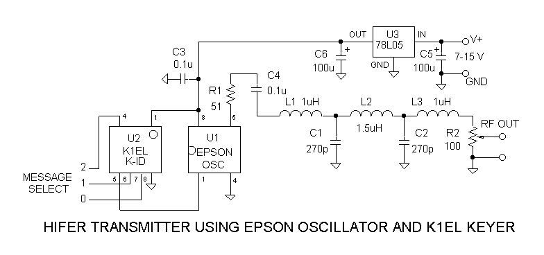
Note that in the diagram, U1 and U2 are shown oriented "nose to nose"; that is, with U2 rotated 180 degrees with respect to U1. This keeps the power and ground connections on the same side of the chips, which makes the layout work better on a solderless breadboard. If you make your own circuit board or use "dead bug" or similar construction, the orientation can be whatever works best for you.
Standard off-the-shelf component values are used in the output filter. PSpice modeling results showing the response when the filter is terminated in a 50-ohm resistive load are shown below. Theoretically there should be little second harmonic content from the square-wave output of the Epson oscillator, and that harmonic falls in the CB band where it would be difficult to observe above the background anyway. The third harmonic is down by the required 60 dB, assuming that your antenna radiates better at the fundamental than at 40.7 MHz.
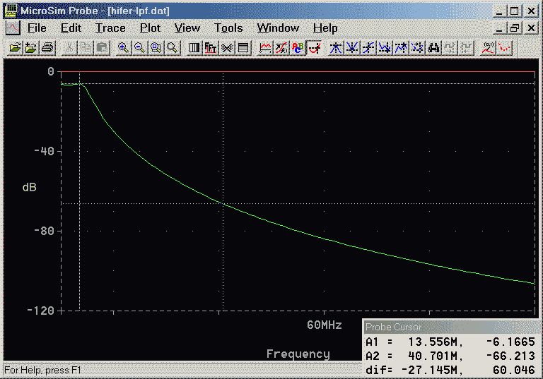
Output Filter Response
Parts list for HiFER transmitter:
C1, C2: 270 pF capacitor -- Digi-Key # 1318PH (sold in quantities of 10)
C3, C4: 0.1 uF capacitor -- Digi-Key # P4924
C5, C6: 100 uF 25V capacitor -- Digi-Key # P5152
L1, L2: 1 uH inductors -- Digi-Key # M7813
L3: 1.5 uH inductor -- Digi-Key # M7815
R1: 51 ohm resistor -- Digi-Key # 51EBK (package of 5)
R2: 100 ohm trimpot -- Digi-Key # 3362P-101
U1: Epson programmable oscillator -- Digi-Key # SG-8002DC-PHB (specify the desired transmit frequency)
U2: K1EL keyer chip (see text)
U3: 78L05 low power 5V regulator -- Digi-Key # 296-1365